This thread has been locked.

If you have a related question, please click the "Ask a related question" button in the top right corner. The newly created question will be automatically linked to this question.

LM5146-Q1: Suitable for my requirement ?

Part Number: LM5146-Q1
Other Parts Discussed in Thread: LM5146, LM5145

Tool/software:

Hello Team, 

I am making a DC - DC converter. Design specifications -

Non isolated

20V - 60V input voltage (nominal - 51.2)

Output voltage - 12V 

Output current requirement - 20A

Ouptut power - 240W

I came accorss LM5146ic but all the ratings and information given in the datasheet are subect to 8A and OCP is at 12A  but in the quick start guide i was able to enter a value of 20A and was still withing range. So is the current limiting based on the MOSFETS ? 

Also in the product details the Iout max was 20A (https://www.ti.com/product/LM5146).

Having a input voltage range higher than my requirement and a sufficiently high output current this seems to be a good fir for my requirement bur

I have attached the filled in excell for the same.

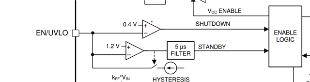
Also for the undervoltage enable logic to function (according to the block diagram given on page 16 of the datasheet) should the voltage on the UVLO pin be 0,4V or 1.2V. From my observation of the quickstart calculation when i give a UVLO of 25V the ratio of the resistors is such that the UVLo pin has 1.18V accorss it so can I assume that 1.2V on the pin measn that the ic enables a lockout ? The what id the 0.4V comparator for shut down mean ? I am assuming that the filter of 5us is a debounce and the voltage needs to be 1.2V at the pin for atleast 5us for the UVLO to work. But is there any way theat we can change the time of debounce ? 

LM5146_quickstart_calculator_revB1.xlsm

Thanks, 

G Karthik

  • Hi Karthik,

    12V/20A should be fine. Just beware of thermal conditions at that high current. Go with Fsw = 250kHz instead of 400kHz, 3.3uH inductance for lower DCR, and 80V FETs (e,g, from onsemi).

    The controller is enabled at 1.2V and is in standby (VCC alive) with EN in the range of ~0.4V to 1.2V.

    Regards,

    Tim

  • Hi Tim,

    Thanks for the reply, can I know the calculations and reasoning done behind arriving at the switching frequency of 250Khz and a 3.3uH inductance ?

    Thanks,

    Karthik.

  • Hi Tim,

    I was looking at the eval board design for the LM5145, optimization of the power stage design(link). As far as ive understood it shows different layouts and the hot loop taken by the switching current in different layout and placement styles. Figure 1 is the least optimal approach that needs to be used as the switching current loop is big and hence higher EMC. Figure 2 - Improved lateral switching loop design is better than figure 1 as the loop now is much smaller than the previous. Then the best approach for minimuising the hot loop would be layout style given in figure 3, the vertically oriented switching loop. 

    In one of my test design I have something similar to figure 2, except for the capacitors being 180 degrees from what is shown in figure 2. So am i right is assumin that this is a bad layout as the switching loop for the current is big.

    Also assuming that I am using the same mosfets, what is the value of the gate resistance i should be having ?

    And in the list of materials i can see that Q1 and Q2 are of different current capabilities so is there any reason why we can go with a nmos with a lower current rating on the high side and a nmos with a higher current rating on the bottom side ?

    Thank you,

    Karthik.

  • Hi Karthik,

    Yes, smaller loop area is always better, but yours looks reasonable. I would go with zero gate resistance (and include a resistor in series with the boot cap as an option).

    If the duty cycle is < 50%, then the high-side FET conducts less than the low-side FET. Thus, the high-side FET can be higher Rdson, lower capacitance, which helps switching losses.

    Regards,

    Tim

  • Hi Tim, 

    1. The boot capacitor that you have mentioned is the one on the BST pin i assume. Include a resistor with the boot cap in series going to the pin of the ic ? Somthing like this ?

    This was given in the TI high density evaluation module - 

    2. Can I know the calculations and reasoning done behind arriving at the switching frequency of 250Khz and a 3.3uH inductance ?

    3. I want to use the Rdson method of current sensing, is there any design conciderations ill have to keep in mind ? Which one is more accurate and recommended ?

    4. If i have a good thermal management system in place and my MOSFETS can handle higher currents then can I go higher on the current, as the modules that are going to be powered by the converter are not yet finalised, so the power requirement might go higher upto 400W as well. Can I go for mosfets in parallel ot higher rated mosfets and use the same control ic ? If yes, the what could be the limit of the output power, would it purely depend on the ability of the mosfets ?

    5. I also wanted to know if a simple pi filter as mentioned on page 34 will do or do we need a robust EMC filtering with common mode filtering, differential mode filtering.

    Thank you,

    Karthik.

  • Hi Karthik,

    !. Yes, a resistor in series with the boot cap.

    2. 250kHz is a good tradeoff of efficiency vs. size. Choose the inductor based on the quickstart calculator recommendation, ~30% ripple current.

    3. Rdson lossless sensing is recommended. See the data sheet for more detail. Use a soft-sat inductor, e.g. powdered iron material.

    4. Yes.

    5. A normal Pi filter (with damping) is often adequate. However, if meeting CISPR 25 Class 5 is the target (up to 108MHz), then a CM choke is often useful.

    Regards,

    Tim