This thread has been locked.

If you have a related question, please click the "Ask a related question" button in the top right corner. The newly created question will be automatically linked to this question.

BQ25120A: Sys out increases to VBAT-threshold

Part Number: BQ25120A

Tool/software:

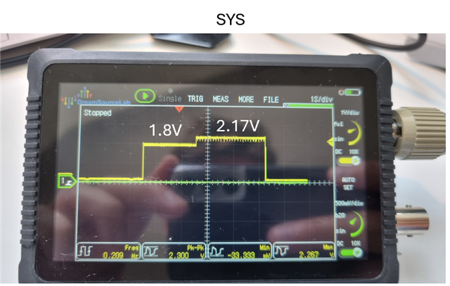
I am struggling to get the sys out to work properly, I want the default 1.8V and it seems to create this for a small period before the voltage suddenly increases to 2.5V (VIN not connected) or 3.6v (VIN connected). It does not seem to be any error messages and these are my register values. I put 0x01 to 0x04 because it generated an VIN_UV after disconnecting the input voltage:
Register 0x00 value: 0x41
Register 0x01 value: 0x04
Register 0x02 value: 0x08
Register 0x03 value: 0x14
Register 0x04 value: 0x0E
Register 0x05 value: 0x78
Register 0x06 value: 0xAA
Register 0x07 value: 0x7C

  • Hi,

    Can you please share your schematics for context?

    Best Regards,

    Juan Ospina

  • Here is the schematic!

  • The problem seem to be when I enable the VDD_3V3_EN as it is 1.8V before that but after this pin goes high the SYS output and LDO output seem to drift and follow vbat

  • Hi Chris,

    Thank you for sharing the schematic. I do have some notes, though they may not necessarily be the cause for the observed behavior:

    - the IN pin should have at least 1 uF capacitance

    Regarding the behavior you mentioned, enabling VDD_3V3_EN should only turn on the LS_LDO rail. What is your VBAT voltage at this time?

    Can you please capture a waveform of the SW node and SYS when the VDD_3V3_EN signal is asserted?

    Best Regards,

    Juan Ospina

  • Hi, I think I solved it now, the main problem seemed to be the timing of the VDD_3V3_EN and writing to the LDO registers. I am not really sure why it did not work earlier cause I thought I wrote the same register values in previous atttempts but must have done something wrong. However I have an additional question, when the LDO turn on it seems to shift the sys out voltage a bit. It should be 1.8V but it is 2.13 when the LDO is turned on (3.3V), it does not affect the circuit as it only powers the MCU and the stable 3.3V is the most important. 

  • Hi Chris,

    I'm not certain why it might cause the rise in voltage. Does the voltage stay high or does it settle back down to 1.8V after some time, and does that timing change when there is a larger load or a smaller load?

    Also, is the LDO operating in LDO mode or Load-Switch mode when it is enabled? One thing we have seen is that the Load Switch being enabled can cause a rapid rush of current from VINLS (usually tied to PMID) to VLSLDO which can cause a very quick drop in PMID voltage and has an impact on SYS output. This can be mitigated by increasing VINLS capacitance, Increasing PMID capacitance, and using the LSLDO in LDO mode rather than Load-Switch mode. If you can provide a capture of SYS, PMID, and LDO when this takes place we can better determine if that is the cause of the behavior.

    Best Regards,

    Juan Ospina

  • Hi, it stays ast 2.1 after the LDO turns on. Here are the graphs for SYS, PMID and LDO. Let me know if anything is unclear or you need more measurements!

  • Hi Chris,

    Would there be a way to capture the SYS waveform in parallel to a SW waveform? I'm trying to identify if, when the 2.17V is present on SYS if the converter is still switching.

    Unless there's an I2C transaction to reconfigure the SYS_VOUT field, it looks like the SYS rail is being overloaded externally. Is there any alternate current paths from the LDO to the SYS rail?

    Best Regards,

    Juan Ospina