This thread has been locked.

If you have a related question, please click the "Ask a related question" button in the top right corner. The newly created question will be automatically linked to this question.

TPS50601A-SP: Jitter ON pulse

Part Number: TPS50601A-SP

Tool/software:

Hello,

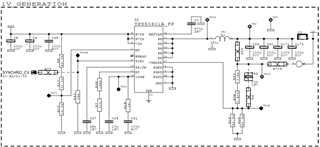
I am using the component to create a 1V from a 6V power supply, and I am facing an issue regarding the pulse ON of the converter which have jitter (around 160ns).

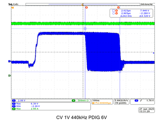
The regulation loop is stable. More than 60° phase margin and 15dB gain margin and the switching frequency is around 440kHz.

The only way to reduce the jitter of the ON pulse is to reduce the input voltage less than 4.5V but it is not acceptable for the project.

Do you have a clue to reduce the jitter ? And why is there so many ? 

L = 10uH and Cout = 4*100uF

Best regards 

Guillaume Bazin 

Electronic Engineer

  • Hi Guillaume,

    Can you please confirm if the scope image you shared above is a single switch pulse (no scope persistence), or an overlay of many cycles (scope persistence turned on)?

    Is the "jitter" inconsistent duty-cycle from pulse-to-pulse?

    I do see your inductor is quite large for your VIN to VOUT, less than 200mA of current ripple. Since this device uses peak current mode control, 10% to 50% current ripple is recommended. I see even at 6A of output current, a 10uH inductor would only provide ~3% current ripple at 6V to 1V. If your output current is small, your ripple current percentage can also be increased to reduce the inductor value.

    It is possible that using a too-large inductor could introduce falling-edge jitter / inconstant duty cycle. Can you try a smaller inductance?

    Please see datasheet section 8.2.2.2 for more information on inductor selection.

    What is your input capacitor (Cin) configuration?

    Thanks,

    Andy

  • The scope is in persistence (overlay of many cycles). 

    Yes the jitter is inconsistent duty cycle from pulse to pulse. 

    Yes i thought also of a reduction of the inductance. So I divided it by two (by addind a second in parallel) but it shows no improvement.

    Cin = 2*100uF + 100nF

    Maybe the slope compensation inside the component is playing a role but it is impossible to change it without changing the frequency. 

    Regards

    Guillaume B

  • Hey Guillaume,

    To put it into perspective we generally suggest around 20-40% current ripple for our products.
    I might suggest something more in the 1 uH range.

    The next thing to go over would be the compensation.
    What equations did you use to create your compensation values?
    Im going through estimates of your crossover frequency and for the most part I think your values may be fine.
    Your CHF is really high though, what is the estimated ESR of your output capacitance network?

    The third thing that it could be is layout related.
    There are a couple of different places where noise injection could cause issues to the device.
    Most notably the COMP, FB, and VIN pins.
    Are the components for COMP/FB on the same side of the board as the pin and are they close to the device?
    Does VIN have decoupling capacitance close to it?
    Are those pins close to any large noise sources?
    Obviously the switcher itself is a noise source, but unless the large circulating currents are routed across the pins, we can neglect it.

    Thanks,
    Daniel