TUSB544: DisplayPort only finishes link training when configured as 4 lane DP with source mode in USB-C DP + USB3 altmode sink device

Part Number: TUSB544
Other Parts Discussed in Thread: TUSB1044, TUSB564

Tool/software:

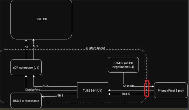
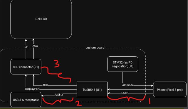
Hi, I have a custom USB-C hub/monitor that connects to a mobile device thru USB-C, and breaks out the DisplayPort signal to a eDP display and the USB3. 1 signal to a USB-A connector. I tried different signal configurations in TUSB544, but I get unexpected results:

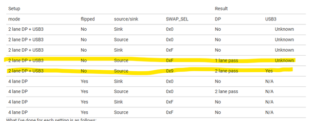
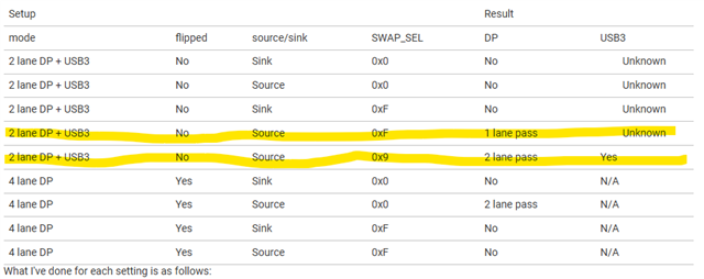
  • 2 lane DP + USB3 in sink mode: USB3 works fine, however DisplayPort can't finish link training (no clock recovery at all; no matter what gain/VOD config I use)
  • 2 lane DP + USB3 in source mode (remember this is a sink device): DP link training fails; most of the time lane 0 can't finish clock recovery, but when it can, it can't finish symbol locking; lane1 always finishes clock recovery and symbol locking. This also doesn't change when I change gain/VOD configs (I didn't test USB3 in this mode)
  • 4 lane DP, flipped, in source mode, and flip AUX lines (so it's in normal orientation): link training finishes, using minimum gain/VOD setting

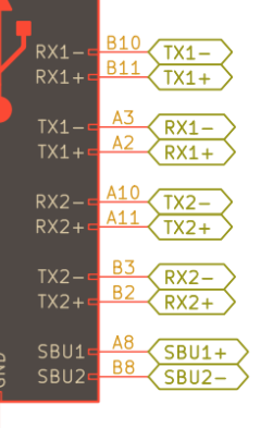
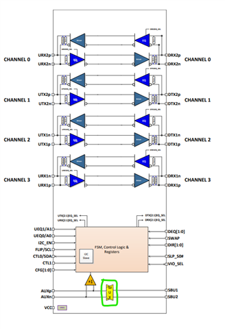
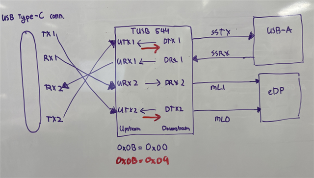
I don't have my schematics at the moment, but from the PCB the lanes are connected as follows:

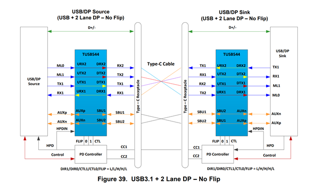
  • USB-C RX2+/- (B2/B3) => UTX1+/-, DTX1+/- => DP1+/-
  • USB-C TX2+/- (A10/A11) => URX1+/-, DRX1+/- => DP0+/-
  • USB-C RX1+/- (A2/A3) => UTX2+/-, DTX2+/- => USB3-A SSTX+/-
  • USB-C TX1+/- (B10/B11) => URX2+/-, DRX2+/- => USB3-A SSRX+/-

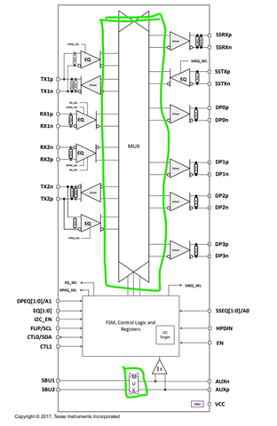
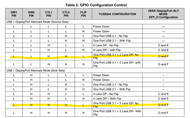
Given this connection, the expected setting should be: CTL[1:0] = 0b11, DIR[1:0] = 0b01, FLIP = 0, SWAP = 0

However, the only setting that worked for me is: CTL[1:0] = 0b10, DIR[1:0] = 0b00, FLIP = 1, SWAP = 0, and set AUX_SBU_OVR = 0b01

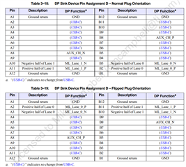
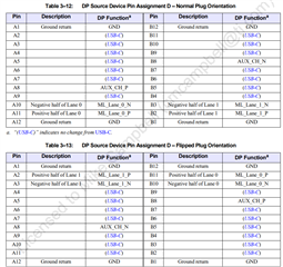
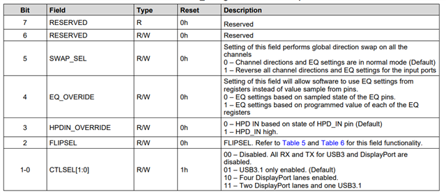
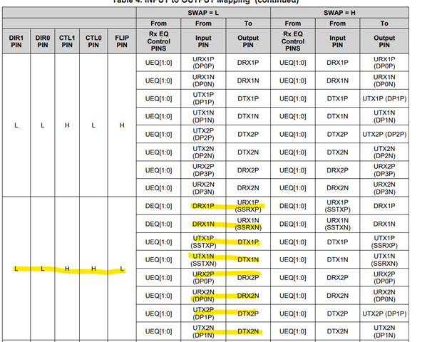
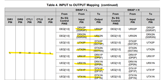
Please let me know what I'm doing wrong. I also would like to know what the sink/source modes in TUSB544 actually change, and how it relates to SWAP, since the datasheet doesn't seem to explain either. The only difference I can observe regarding sink/source modes is in Table 4 of the datasheet, is whether e.g. DP0P/N markings appear on the input or output side. Thanks in advance! 

  • Hi,

    Looking into this now

  • We need to confirm a few things.

    1) Can you capture an aux log for the link training

    2) Can you confirm that in this embedded application the eDP display is able to handle DP scrambling seeds? Are you bale to enable/ disable ASSR?

    3) What are the pull ups and pull downs on the AUX bus? There are different connections for source and sink mode operation.

    SWAP relates to the path of EQ. By default it goes from Upstream to Downstream connection UTX/URX -> DTX/DRX, when swap is enabled, the EQ path goes from downstream to upstream DTX/DRX -> UTX/URX.

  • 1) The captured AUX logs is as follows ([] indicates length (or unknown register), data after ACK is in hex):

    For a failed training (this is the expected config, 2 lane DP + USB3 sink):

    dp_aux-1: AUX Read DPCD_REV [1] -> ACK 11
    dp_aux-1: AUX Read DPCD_REV [16] -> ACK 110a8241000001400202000000030000
    dp_aux-1: AUX Read DPCD_REV [1] -> ACK 11
    dp_aux-1: AUX Read [0x90] [1] -> ACK 00
    dp_aux-1: AUX Read DPCD_REV [1] -> ACK 11
    dp_aux-1: AUX Read [0x60] [16] -> ACK 00000000000000000000000000000000
    dp_aux-1: AUX Read PSR_SUPPORT [1] -> ACK 00
    dp_aux-1: AUX Read DPCD_REV [1] -> ACK 11
    dp_aux-1: AUX Read SET_POWER [1] -> ACK 01
    dp_aux-1: AUX Write SET_POWER = 01 -> ACK
    dp_aux-1: AUX Read DPCD_REV [1] -> ACK 11
    dp_aux-1: AUX Read SINK_COUNT [1] -> ACK 41
    dp_aux-1: AUX Write TRAINING_PATTERN_SET = 00 -> ACK
    dp_aux-1: AUX Write LINK_BW_SET = 0a -> ACK
    dp_aux-1: AUX Write LANE_COUNT_SET = 82 -> ACK
    dp_aux-1: AUX Write DOWNSPREAD_CTRL = 10 -> ACK
    dp_aux-1: AUX Write MAIN_LINK_CHANNEL_CODING_SET = 01 -> ACK
    dp_aux-1: AUX Write TRAINING_PATTERN_SET = 21 -> ACK
    dp_aux-1: AUX Write TRAINING_LANE0_SET = 0000 -> ACK
    dp_aux-1: AUX Read DPCD_REV [1] -> ACK 11
    dp_aux-1: AUX Read LANE0_1_STATUS [6] -> ACK 000080021100
    dp_aux-1: AUX Write TRAINING_LANE0_SET = 0101 -> ACK
    dp_aux-1: AUX Read DPCD_REV [1] -> ACK 11
    dp_aux-1: AUX Read LANE0_1_STATUS [6] -> ACK 000080022200
    dp_aux-1: AUX Write TRAINING_LANE0_SET = 0202 -> ACK
    dp_aux-1: AUX Read DPCD_REV [1] -> ACK 11
    dp_aux-1: AUX Read LANE0_1_STATUS [6] -> ACK 000080023300
    dp_aux-1: AUX Write TRAINING_LANE0_SET = 0707 -> ACK
    dp_aux-1: AUX Read DPCD_REV [1] -> ACK 11
    dp_aux-1: AUX Read LANE0_1_STATUS [6] -> ACK 000080020000
    dp_aux-1: AUX Write TRAINING_LANE0_SET = 0000 -> ACK
    dp_aux-1: AUX Read DPCD_REV [1] -> ACK 11
    dp_aux-1: AUX Read LANE0_1_STATUS [6] -> ACK 000080020000
    dp_aux-1: AUX Write TRAINING_LANE0_SET = 0000 -> ACK
    dp_aux-1: AUX Read DPCD_REV [1] -> ACK 11
    dp_aux-1: AUX Read LANE0_1_STATUS [6] -> ACK 000080020000
    dp_aux-1: AUX Write TRAINING_LANE0_SET = 0000 -> ACK
    dp_aux-1: AUX Read DPCD_REV [1] -> ACK 11
    dp_aux-1: AUX Read LANE0_1_STATUS [6] -> ACK 000080020000
    dp_aux-1: AUX Write TRAINING_LANE0_SET = 0000 -> ACK
    dp_aux-1: AUX Read DPCD_REV [1] -> ACK 11
    dp_aux-1: AUX Read LANE0_1_STATUS [6] -> ACK 000080020000
    dp_aux-1: AUX Write TRAINING_LANE0_SET = 0000 -> ACK
    dp_aux-1: AUX Read DPCD_REV [1] -> ACK 11
    dp_aux-1: AUX Read LANE0_1_STATUS [6] -> ACK 000080020000
    dp_aux-1: AUX Write TRAINING_PATTERN_SET = 00 -> ACK
    dp_aux-1: AUX Write LINK_BW_SET = 06 -> ACK
    dp_aux-1: AUX Write LANE_COUNT_SET = 82 -> ACK
    dp_aux-1: AUX Write DOWNSPREAD_CTRL = 10 -> ACK
    dp_aux-1: AUX Write MAIN_LINK_CHANNEL_CODING_SET = 01 -> ACK
    dp_aux-1: AUX Write TRAINING_PATTERN_SET = 21 -> ACK
    dp_aux-1: AUX Write TRAINING_LANE0_SET = 0000 -> ACK
    dp_aux-1: AUX Read DPCD_REV [1] -> ACK 11
    dp_aux-1: AUX Read LANE0_1_STATUS [6] -> ACK 000080020000
    dp_aux-1: AUX Write TRAINING_LANE0_SET = 0000 -> ACK
    dp_aux-1: AUX Read DPCD_REV [1] -> ACK 11
    dp_aux-1: AUX Read LANE0_1_STATUS [6] -> ACK 000080020000
    dp_aux-1: AUX Write TRAINING_LANE0_SET = 0000 -> ACK
    dp_aux-1: AUX Read DPCD_REV [1] -> ACK 11
    dp_aux-1: AUX Read LANE0_1_STATUS [6] -> ACK 000080020000
    dp_aux-1: AUX Write TRAINING_LANE0_SET = 0000 -> ACK
    dp_aux-1: AUX Read DPCD_REV [1] -> ACK 11
    dp_aux-1: AUX Read LANE0_1_STATUS [6] -> ACK 000080020000
    dp_aux-1: AUX Write TRAINING_LANE0_SET = 0000 -> ACK
    dp_aux-1: AUX Read DPCD_REV [1] -> ACK 11
    dp_aux-1: AUX Read LANE0_1_STATUS [6] -> ACK 000080020000
    dp_aux-1: AUX Write TRAINING_PATTERN_SET = 00 -> ACK
    dp_aux-1: AUX Write LINK_BW_SET = 0a -> ACK
    dp_aux-1: AUX Write LANE_COUNT_SET = 81 -> ACK
    dp_aux-1: AUX Write DOWNSPREAD_CTRL = 10 -> ACK
    dp_aux-1: AUX Write MAIN_LINK_CHANNEL_CODING_SET = 01 -> ACK
    dp_aux-1: AUX Write TRAINING_PATTERN_SET = 21 -> ACK
    dp_aux-1: AUX Write TRAINING_LANE0_SET = 00 -> ACK
    dp_aux-1: AUX Read DPCD_REV [1] -> ACK 11
    dp_aux-1: AUX Read LANE0_1_STATUS [6] -> ACK 000080020000
    dp_aux-1: AUX Write TRAINING_LANE0_SET = 00 -> ACK
    dp_aux-1: AUX Read DPCD_REV [1] -> ACK 11
    dp_aux-1: AUX Read LANE0_1_STATUS [6] -> ACK 000080020000
    dp_aux-1: AUX Write TRAINING_LANE0_SET = 00 -> ACK
    dp_aux-1: AUX Read DPCD_REV [1] -> ACK 11
    dp_aux-1: AUX Read LANE0_1_STATUS [6] -> ACK 000080020000
    dp_aux-1: AUX Write TRAINING_LANE0_SET = 00 -> ACK
    dp_aux-1: AUX Read DPCD_REV [1] -> ACK 11
    dp_aux-1: AUX Read LANE0_1_STATUS [6] -> ACK 000080020000
    dp_aux-1: AUX Write TRAINING_LANE0_SET = 00 -> ACK
    dp_aux-1: AUX Read DPCD_REV [1] -> ACK 11
    dp_aux-1: AUX Read LANE0_1_STATUS [6] -> ACK 000080020000
    dp_aux-1: AUX Write TRAINING_PATTERN_SET = 00 -> ACK
    dp_aux-1: AUX Write LINK_BW_SET = 06 -> ACK
    dp_aux-1: AUX Write LANE_COUNT_SET = 81 -> ACK
    dp_aux-1: AUX Write DOWNSPREAD_CTRL = 10 -> ACK
    dp_aux-1: AUX Write MAIN_LINK_CHANNEL_CODING_SET = 01 -> ACK
    dp_aux-1: AUX Write TRAINING_PATTERN_SET = 21 -> ACK
    dp_aux-1: AUX Write TRAINING_LANE0_SET = 00 -> ACK
    dp_aux-1: AUX Read DPCD_REV [1] -> ACK 11
    dp_aux-1: AUX Read LANE0_1_STATUS [6] -> ACK 000080020000
    dp_aux-1: AUX Write TRAINING_LANE0_SET = 00 -> ACK
    dp_aux-1: AUX Read DPCD_REV [1] -> ACK 11
    dp_aux-1: AUX Read LANE0_1_STATUS [6] -> ACK 000080020000
    dp_aux-1: AUX Write TRAINING_LANE0_SET = 00 -> ACK
    dp_aux-1: AUX Read DPCD_REV [1] -> ACK 11
    dp_aux-1: AUX Read LANE0_1_STATUS [6] -> ACK 000080020000
    dp_aux-1: AUX Write TRAINING_LANE0_SET = 00 -> ACK
    dp_aux-1: AUX Read DPCD_REV [1] -> ACK 11
    dp_aux-1: AUX Read LANE0_1_STATUS [6] -> ACK 000080020000
    dp_aux-1: AUX Write TRAINING_LANE0_SET = 00 -> ACK
    dp_aux-1: AUX Read DPCD_REV [1] -> ACK 11
    dp_aux-1: AUX Read LANE0_1_STATUS [6] -> ACK 000080020000
    dp_aux-1: AUX Write TRAINING_PATTERN_SET = 00 -> ACK

    For a successful training (using 4 lane DP in source mode):

    dp_aux-1: AUX Read DPCD_REV [1] -> ACK 11
    dp_aux-1: AUX Read DPCD_REV [16] -> ACK 110a8241000001400202000000030000
    dp_aux-1: AUX Read DPCD_REV [1] -> ACK 11
    dp_aux-1: AUX Read [0x90] [1] -> ACK 00
    dp_aux-1: AUX Read DPCD_REV [1] -> ACK 11
    dp_aux-1: AUX Read [0x60] [16] -> ACK 00000000000000000000000000000000
    dp_aux-1: AUX Read PSR_SUPPORT [1] -> ACK 00
    dp_aux-1: AUX Read DPCD_REV [1] -> ACK 11
    dp_aux-1: AUX Read SET_POWER [1] -> ACK 01
    dp_aux-1: AUX Write SET_POWER = 01 -> ACK
    dp_aux-1: AUX Read DPCD_REV [1] -> ACK 11
    dp_aux-1: AUX Read SINK_COUNT [1] -> ACK 41
    dp_aux-1: AUX Write TRAINING_PATTERN_SET = 00 -> ACK
    dp_aux-1: AUX Write LINK_BW_SET = 0a -> ACK
    dp_aux-1: AUX Write LANE_COUNT_SET = 82 -> ACK
    dp_aux-1: AUX Write DOWNSPREAD_CTRL = 10 -> ACK
    dp_aux-1: AUX Write MAIN_LINK_CHANNEL_CODING_SET = 01 -> ACK
    dp_aux-1: AUX Write TRAINING_PATTERN_SET = 21 -> ACK
    dp_aux-1: AUX Write TRAINING_LANE0_SET = 0000 -> ACK
    dp_aux-1: AUX Read DPCD_REV [1] -> ACK 11
    dp_aux-1: AUX Read LANE0_1_STATUS [6] -> ACK 110080020000
    dp_aux-1: AUX Write TRAINING_PATTERN_SET = 22 -> ACK
    dp_aux-1: AUX Write TRAINING_LANE0_SET = 0000 -> ACK
    dp_aux-1: AUX Read DPCD_REV [1] -> ACK 11
    dp_aux-1: AUX Read LANE0_1_STATUS [6] -> ACK 770081020000
    dp_aux-1: AUX Write TRAINING_PATTERN_SET = 00 -> ACK
    dp_aux-1: I2C MOT Write 0x30 = 00 -> ACK
    dp_aux-1: I2C MOT Write 0x50 = 00 -> ACK
    dp_aux-1: I2C MOT Read 0x50 [16] -> ACK 00ffffffffffff000daee51400000000
    dp_aux-1: I2C MOT Read 0x50 [16] -> ACK 041c0104a51f1178020865975b548e27
    dp_aux-1: I2C MOT Read 0x50 [16] -> ACK 1e505400000001010101010101010101
    dp_aux-1: I2C MOT Read 0x50 [16] -> ACK 010101010101b43b804a71383440503c
    dp_aux-1: I2C MOT Read 0x50 [16] -> ACK 680035ad10000018000000fe004e3134
    dp_aux-1: I2C MOT Read 0x50 [16] -> ACK 304847412d4541310a20000000fe0043
    dp_aux-1: I2C MOT Read 0x50 [16] -> ACK 4d4e0a202020202020202020000000fe
    dp_aux-1: I2C MOT Read 0x50 [16] -> ACK 004e3134304847412d4541310a20004c
    dp_aux-1: I2C Read 0x50 -> ACK
    dp_aux-1: AUX Read DPCD_REV [1] -> ACK 11
    dp_aux-1: AUX Read SINK_COUNT [1] -> ACK 41
    dp_aux-1: AUX Read DPCD_REV [1] -> ACK 11
    dp_aux-1: AUX Read DEVICE_SERVICE_IRQ_VECTOR [1] -> ACK 00
    dp_aux-1: AUX Read DPCD_REV [1] -> ACK 11
    dp_aux-1: AUX Read LANE0_1_STATUS [6] -> ACK 770001010000

    2) I'm not sure about those. I don't have a DP AUX transceiver, I'm just observing AUX traffic between the source and sink

    3) The pull resistors should be as the datasheet for sink operation. On the board, I have 2M pulldowns on the SBU pins, and 1M pull down on AUX-, 1M pull up on AUX+ near the TUSB544 before the AC coupling caps

  • Hi,

    Can you share a schematic of your system?

  • I should also mention that, during DisplayPort VDMs, I'm always advertising as a UFP only supporting pin assignment D

  • Hi Steven,

    Can you clarify if this is a DP at mode source or sink application? We typically do not see a DP source in the UFP orientation.

    I will try to have the schematic review ready in 1-2 days.

  • The board is designed to be a DP sink

  • How are we testing it as a DP src here?

    For a successful training (using 4 lane DP in source mode):
  • What are the trace lengths on the board and what are the EQ values used?

  • Well that's the weird thing, I've only used the board in sink mode, yet link training only succeeds in source mode

  • Trace lengths on the board are around 1in on both sides of the TUSB544, though from the eDP connector to display it's around 3in. When using source mode on the TUSB544, training can be passed with minimum EQ settings. When using sink mode (and thus training doesn't pass), none of the EQ values work 

  • How are we testing it as a DP src here?

    Oh sorry I missed the "how" part of the question. Everything else on the board/firmware is left as the same, connected to a eDP display (so sink) and advertises as a UFP supporting pin assignment D. Only the TUSB544 configuration changes to source mode (and using 4 lane DP, in flipped orientation)

  • Hi Steven,

    How much EQ does the SoC have? Are we able to tune this value?

    How is the SoC addressing the differences in pinouts for SRC mode and SNK mode?

    Lane 0 and lane 1 are swapped in SNK vs. SRC applications. 

    I dont believe this is an EQ issue with the TUSB1044, especially because it works properly in SRC mode. However, this issue may be with the direction it is applied. If possible can you place a pull up on the SWAP pin to reverse the direction of the EQ applied. 

    Try testing with SWAP pulled up. and see if we see more progress in link training results.

  • How much EQ does the SoC have? Are we able to tune this value?

    I'm not sure. This is simply my phone (not development hardware). I also don't have any equipment to test this value (if it's even testable) 

    Try testing with SWAP pulled up. and see if we see more progress in link training results.

    With sink mode in 2 lane DP configuration you mean? Sure I can try to test that

  • Also, it'll be pretty weird if it's a pinout issue: the USB3 works in pin configuration D, just not the DP

  • One more thing: I've been using the I2C mode, and whenever I'm setting EQ values I'm setting the upstream and downstream EQs of each lane to be the same, so I doubt setting SWAP is gonna make a difference. But I will test that (a bit later)

  • Alright, I did some simple testing with SWAP (actually setting the SWAP_SEL register to 0xf since I'm using I2C).

    • 2 lane DP + USB3 in unflipped sink mode: setting SWAP still fails link training
    • 4 lane DP in flipped source mode (known passing config): setting SWAP also fails link training
      • but, if SWAP flips channel direction, then 4 lane DP in flipped sink mode setting SWAP should give the same result. But it also fails link training 
  • Hmm. 2 lane DP + USB3 in unflipped source mode with SWAP set does pass training on lane 0 (though the display doesn't seem to support this and is blank):

    dp_aux-1: AUX Read DPCD_REV [1] -> ACK 11
    dp_aux-1: AUX Read DPCD_REV [16] -> ACK 110a8241000001400202000000030000
    dp_aux-1: AUX Read DPCD_REV [1] -> ACK 11
    dp_aux-1: AUX Read [0x90] [1] -> ACK 00
    dp_aux-1: AUX Read DPCD_REV [1] -> ACK 11
    dp_aux-1: AUX Read [0x60] [16] -> ACK 00000000000000000000000000000000
    dp_aux-1: AUX Read PSR_SUPPORT [1] -> ACK 00
    dp_aux-1: AUX Read DPCD_REV [1] -> ACK 11
    dp_aux-1: AUX Read SET_POWER [1] -> ACK 01
    dp_aux-1: AUX Write SET_POWER = 01 -> ACK
    dp_aux-1: AUX Read DPCD_REV [1] -> ACK 11
    dp_aux-1: AUX Read SINK_COUNT [1] -> ACK 41
    dp_aux-1: AUX Write TRAINING_PATTERN_SET = 00 -> ACK
    dp_aux-1: AUX Write LINK_BW_SET = 0a -> ACK
    dp_aux-1: AUX Write LANE_COUNT_SET = 82 -> ACK
    dp_aux-1: AUX Write DOWNSPREAD_CTRL = 10 -> ACK
    dp_aux-1: AUX Write MAIN_LINK_CHANNEL_CODING_SET = 01 -> ACK
    dp_aux-1: AUX Write TRAINING_PATTERN_SET = 21 -> ACK
    dp_aux-1: AUX Write TRAINING_LANE0_SET = 0000 -> ACK
    dp_aux-1: AUX Read DPCD_REV [1] -> ACK 11
    dp_aux-1: AUX Read LANE0_1_STATUS [6] -> ACK 010080021100
    dp_aux-1: AUX Write TRAINING_LANE0_SET = 0101 -> ACK
    dp_aux-1: AUX Read DPCD_REV [1] -> ACK 11
    dp_aux-1: AUX Read LANE0_1_STATUS [6] -> ACK 010080022200
    dp_aux-1: AUX Write TRAINING_LANE0_SET = 0202 -> ACK
    dp_aux-1: AUX Read DPCD_REV [1] -> ACK 11
    dp_aux-1: AUX Read LANE0_1_STATUS [6] -> ACK 010080023300
    dp_aux-1: AUX Write TRAINING_LANE0_SET = 0707 -> ACK
    dp_aux-1: AUX Read DPCD_REV [1] -> ACK 11
    dp_aux-1: AUX Read LANE0_1_STATUS [6] -> ACK 010080020000
    dp_aux-1: AUX Write TRAINING_LANE0_SET = 0000 -> ACK
    dp_aux-1: AUX Read DPCD_REV [1] -> ACK 11
    dp_aux-1: AUX Read LANE0_1_STATUS [6] -> ACK 010080020000
    dp_aux-1: AUX Write TRAINING_LANE0_SET = 0000 -> ACK
    dp_aux-1: AUX Read DPCD_REV [1] -> ACK 11
    dp_aux-1: AUX Read LANE0_1_STATUS [6] -> ACK 010080020000
    dp_aux-1: AUX Write TRAINING_LANE0_SET = 0000 -> ACK
    dp_aux-1: AUX Read DPCD_REV [1] -> ACK 11
    dp_aux-1: AUX Read LANE0_1_STATUS [6] -> ACK 010080020000
    dp_aux-1: AUX Write TRAINING_LANE0_SET = 0000 -> ACK
    dp_aux-1: AUX Read DPCD_REV [1] -> ACK 11
    dp_aux-1: AUX Read LANE0_1_STATUS [6] -> ACK 010080020000
    dp_aux-1: AUX Write TRAINING_LANE0_SET = 0000 -> ACK
    dp_aux-1: AUX Read DPCD_REV [1] -> ACK 11
    dp_aux-1: AUX Read LANE0_1_STATUS [6] -> ACK 010080020000
    dp_aux-1: AUX Write TRAINING_PATTERN_SET = 00 -> ACK
    dp_aux-1: AUX Write LINK_BW_SET = 06 -> ACK
    dp_aux-1: AUX Write LANE_COUNT_SET = 82 -> ACK
    dp_aux-1: AUX Write DOWNSPREAD_CTRL = 10 -> ACK
    dp_aux-1: AUX Write MAIN_LINK_CHANNEL_CODING_SET = 01 -> ACK
    dp_aux-1: AUX Write TRAINING_PATTERN_SET = 21 -> ACK
    dp_aux-1: AUX Write TRAINING_LANE0_SET = 0000 -> ACK
    dp_aux-1: AUX Read DPCD_REV [1] -> ACK 11
    dp_aux-1: AUX Read LANE0_1_STATUS [6] -> ACK 010080020000
    dp_aux-1: AUX Write TRAINING_LANE0_SET = 0000 -> ACK
    dp_aux-1: AUX Read DPCD_REV [1] -> ACK 11
    dp_aux-1: AUX Read LANE0_1_STATUS [6] -> ACK 010080020000
    dp_aux-1: AUX Write TRAINING_LANE0_SET = 0000 -> ACK
    dp_aux-1: AUX Read DPCD_REV [1] -> ACK 11
    dp_aux-1: AUX Read LANE0_1_STATUS [6] -> ACK 010080020000
    dp_aux-1: AUX Write TRAINING_LANE0_SET = 0000 -> ACK
    dp_aux-1: AUX Read DPCD_REV [1] -> ACK 11
    dp_aux-1: AUX Read LANE0_1_STATUS [6] -> ACK 010080020000
    dp_aux-1: AUX Write TRAINING_LANE0_SET = 0000 -> ACK
    dp_aux-1: AUX Read DPCD_REV [1] -> ACK 11
    dp_aux-1: AUX Read LANE0_1_STATUS [6] -> ACK 010080020000
    dp_aux-1: AUX Write TRAINING_PATTERN_SET = 00 -> ACK
    dp_aux-1: AUX Write LINK_BW_SET = 0a -> ACK
    dp_aux-1: AUX Write LANE_COUNT_SET = 81 -> ACK
    dp_aux-1: AUX Write DOWNSPREAD_CTRL = 10 -> ACK
    dp_aux-1: AUX Write MAIN_LINK_CHANNEL_CODING_SET = 01 -> ACK
    dp_aux-1: AUX Write TRAINING_PATTERN_SET = 21 -> ACK
    dp_aux-1: AUX Write TRAINING_LANE0_SET = 00 -> ACK
    dp_aux-1: AUX Read DPCD_REV [1] -> ACK 11
    dp_aux-1: AUX Read LANE0_1_STATUS [6] -> ACK 010080020000
    dp_aux-1: AUX Write TRAINING_PATTERN_SET = 22 -> ACK
    dp_aux-1: AUX Write TRAINING_LANE0_SET = 00 -> ACK
    dp_aux-1: AUX Read DPCD_REV [1] -> ACK 11
    dp_aux-1: AUX Read LANE0_1_STATUS [6] -> ACK 070081020000
    dp_aux-1: AUX Write TRAINING_PATTERN_SET = 00 -> ACK
    dp_aux-1: I2C MOT Write 0x30 = 00 -> ACK
    dp_aux-1: I2C MOT Write 0x50 = 00 -> ACK
    dp_aux-1: I2C MOT Read 0x50 [16] -> ACK 00ffffffffffff000daee51400000000
    dp_aux-1: I2C MOT Read 0x50 [16] -> ACK 041c0104a51f1178020865975b548e27
    dp_aux-1: I2C MOT Read 0x50 [16] -> ACK 1e505400000001010101010101010101
    dp_aux-1: I2C MOT Read 0x50 [16] -> ACK 010101010101b43b804a71383440503c
    dp_aux-1: I2C MOT Read 0x50 [16] -> ACK 680035ad10000018000000fe004e3134
    dp_aux-1: I2C MOT Read 0x50 [16] -> ACK 304847412d4541310a20000000fe0043
    dp_aux-1: I2C MOT Read 0x50 [16] -> ACK 4d4e0a202020202020202020000000fe
    dp_aux-1: I2C MOT Read 0x50 [16] -> ACK 004e3134304847412d4541310a20004c
    dp_aux-1: I2C Read 0x50 -> ACK
    dp_aux-1: AUX Read DPCD_REV [1] -> ACK 11
    dp_aux-1: AUX Read DEVICE_SERVICE_IRQ_VECTOR [1] -> ACK 00
    dp_aux-1: AUX Read DPCD_REV [1] -> ACK 11
    dp_aux-1: AUX Read SINK_COUNT [1] -> ACK 41
    dp_aux-1: AUX Read DPCD_REV [1] -> ACK 11
    dp_aux-1: AUX Read DEVICE_SERVICE_IRQ_VECTOR [1] -> ACK 00
    dp_aux-1: AUX Write DEVICE_SERVICE_IRQ_VECTOR = 00 -> ACK
    dp_aux-1: AUX Read DPCD_REV [1] -> ACK 11
    dp_aux-1: AUX Read LANE0_1_STATUS [6] -> ACK 070001000000

  • More interesting: 2 lane DP + USB3 in unflipped source mode with SWAP_SEL set to 0x8 (i.e. flipping only one of the lanes) passes link training on both lanes. USB3 doesn't work however

  •  Okay. 2 lane DP + USB3 in unflipped source mode with SWAP_SEL set to 0x9 (i.e. swapping DP lane 0 and USB3 SSRX lane) passes DP link training on both lanes and USB3 works. While this enables the full functionality of the board, it still kinda doesn't answer the actual question: why does it work under such weird configurations?

  • Hi Steven,

    I'm struggling to follow what tests are being done and what tests have passed. Could you make a table of sorts showing what works and doesn't work?

    It seems we are able to pass in source configuration with some adjusting of the direction of EQ. 

    Do we have any info on sink mode with swap?

  • Hi,

    I'm closing this thread due to inactivity.

  • Sorry, with the forum downtime being on the weekend I didn't have time to reply to this.

    Here's a table of what I've tested:

    Setup Result
    mode flipped source/sink SWAP_SEL DP USB3
    2 lane DP + USB3 No Sink 0x0 No Unknown
    2 lane DP + USB3 No Source 0x0 No Unknown
    2 lane DP + USB3 No Sink 0xF No Unknown
    2 lane DP + USB3 No Source 0xF 1 lane pass Unknown
    2 lane DP + USB3 No Source 0x9 2 lane pass Yes
    4 lane DP Yes Sink 0x0 No N/A
    4 lane DP Yes Source 0x0 2 lane pass N/A
    4 lane DP Yes Sink 0xF No N/A
    4 lane DP Yes Source 0xF No N/A

    What I've done for each setting is as follows:

    • 4 lane DP => CTLSEL = 0b10
    • 2 lane DP + USB3 => CTLSEL = 0b11
    • Source => DIR_SEL = 0b00
    • Sink => DIR_SEL = 0b01
    • Setting flip for 4 lane DP => FLIPSEL = 1, AUX_SBU_OVR = 0b01

    Hopefully this makes it clearer what I've tried

  • Hi Steven,

    Are you able to run compliance on this port?

    Can you test this with register with and without HPDIN override and EQ override?

    Also what is the EQ setting used per lane?

    Can you share a schematic/ layout?

  • Are you able to run compliance on this port?

    What do you mean by this? I'm probably not able to, since I don't have any equipment to measure/look at eye diagrams

    Can you test this with register with and without HPDIN override and EQ override?

    I've been using HPDIN and EQ overrides for above testing, but if I unset HPDIN and EQ overrides (EQ pins left floating) there's no difference in the results for the highlighted rows. 

    Also what is the EQ setting used per lane?

    It doesn't seem to matter in either the failing or passing cases. Setting EQ to max in failing setup still fails, and setting EQ to min in passing setup passes with minimum pre-emphasis/voltage swing in link training

    Can you share a schematic/ layout?

    I've already shared the schematics above

  • Are you able to run compliance on this port?

    What do you mean by this? I'm probably not able to, since I don't have any equipment to measure/look at eye diagrams

    Gotcha, this will make debugging a little more difficult.

    Can you test this with register with and without HPDIN override and EQ override?

    I've been using HPDIN and EQ overrides for above testing, but if I unset HPDIN and EQ overrides (EQ pins left floating) there's no difference in the results for the highlighted rows. 

    OK

    Also what is the EQ setting used per lane?

    It doesn't seem to matter in either the failing or passing cases. Setting EQ to max in failing setup still fails, and setting EQ to min in passing setup passes with minimum pre-emphasis/voltage swing in link training

    What EQ values have been tested? Just the max and min? 

    Can you share a schematic/ layout?

    I've already shared the schematics above

    The schematic shared seems to be a daughtercard. Is there any way I could see the whole picture including the MB?

  • I see you are using the TUSB544 as the redriver facing the connector, but you need an alt. mode mux to separate the video paths from the USB paths. Do you have an alt. mode mux in the signal path?

    The pinout from the TUSB544 to the USB-C connector is also incorrect. 

    TX1, TX2, Rx1, and RX2 should be plugged into TX1, TX2, RX1, and RX2 respectively.

    However, the are not routed this way

    I believe the part you are looking for is the TUSB564 rather than the TUSB544. Because this allows you to separate the USB and video signal using a crossbar mux. The TUSB544 does not have this functionality.

  • I see you are using the TUSB544 as the redriver facing the connector, but you need an alt. mode mux to separate the video paths from the USB paths.

    Why is that needed? Aren't the DP lanes already separate from the USB 3 lanes?

    Also, both TUSB544 and TUSB564 says they are muxes already (the TUSB564 just breaks out the USB 3 signals to their own pins), so what's the difference there? 

    If I do need another mux, how come this following configuration work without any issues?

    2 lane DP + USB3 No Source 0x9 2 lane pass Yes

    The pinout from the TUSB544 to the USB-C connector is also incorrect. 

    That is deliberately flipped, as the signals will go straight into a USB-C plug, so I need to reorder the pins myself. 

  • Hi Steven,

    Why is that needed? Aren't the DP lanes already separate from the USB 3 lanes?

    Also, both TUSB544 and TUSB564 says they are muxes already (the TUSB564 just breaks out the USB 3 signals to their own pins), so what's the difference there? 

    Without a mux to route the signal correctly only one of the normal and flip orientations will work. 

    Ex)

    normal orientation TX1 -> SSTX, RX1 -> SSRX, TX2 -> DP0, RX2 -> DP1

    flip orientation: TX1-> DP0, RX1 -> DP1, TX2 ->SSTX, RX2 -> SSRX

    Without a cross-bar mux to route the flipped orientation to the correct receivers, the DP signal will go to USB receiver, and the USB signals will go to DP receivers. 

    The TUSB544 operates as a redriver with no crossbar mux capabilities. It only has a mux for the SBU and AUX pins.

    The TUSB564 incorporates a crossbar mux while having redriving capabilities. 

    If I do need another mux, how come this following configuration work without any issues?

    2 lane DP + USB3 No Source 0x9 2 lane pass Yes

    Without a crossbar MUX only certain orientations will work.

    normal orientation USB only, normal orientation 2xDP 1xUSB will work, only 2 lanes in 4lane DP mode in normal and flip.

    All other orientations will not work correctly.

    Please see the TUSB564 EVM for reference: https://www.ti.com/tool/TUSB564RNQEVM

    The schematics can be found in the users guide: https://www.ti.com/lit/pdf/sllu279

  • Without a crossbar MUX only certain orientations will work.

    normal orientation USB only, normal orientation 2xDP 1xUSB will work, only 2 lanes in 4lane DP mode in normal and flip.

    I see, thanks for the explanation! However, since on my board the TUSB544 is connected to a USB-C plug directly, there'll only ever be one orientation from the perspective of the TUSB544. And, the board should be designed in such a way that 2 lane DP and USB3 should just work in the "normal" orientation (again, due to the plug, there won't be a flipped orientation). 

    I could try a TUSB564 in my next design, but for the current board, my question is still not answered 

  • Hi Steven,

    Its difficult to isolate the issue without eye diagrams and data to analyze. Sorry this debug it taking so long.

    Are you able to share the rest of the schematic or a block diagram of the test setup? Especially between source testing and sink testing.

    From what I understand in this system The DP path is hardwired to be only on the TX2 and RX2 path, and the USB path is hardwired to be on the TX1 and RX1 path. 

    This looks to be the pin assignment that is being used. 

    Could clarify what you mean by these values? The register I'm assuming you are writing to is 0x0A:

    In the settings where we have a passing result. If register 0x0A is 0x09, then we would be disabling the part. 

    And if 0x0A is 0x0F, then flip would be enabled. If possible can you share the register address and the data read from it?

  • Its difficult to isolate the issue without eye diagrams and data to analyze. Sorry this debug it taking so long.

    Sorry. I'll try to ask around to see if I can find any such equipment..

    Are you able to share the rest of the schematic or a block diagram of the test setup? Especially between source testing and sink testing.

    I don't think I have anything else to share. J1 (the pin header) in the top left of the schematics just connects to a eDP display, and P1 (the USB-C plug) just connects to my phone/laptop directly.

    This looks to be the pin assignment that is being used. 

    That's correct, pin assignment D

    Could clarify what you mean by these values? The register I'm assuming you are writing to is 0x0A:

    Oops, mistake on my part: this is supposed to be the field CH_SWAP_SEL, in General_2 register (offset 0x0B). I've never actually set the SWAP_SEL bit in the General_1 register (offset 0x0A)

  • Ah gotcha. 

    The signal path should look as follows for the sink path.

    Can you share the register settings of 0x0A when these tests were being done?

    First thing I want to check is continuity. Can we probe the signal paths and make sure they are routed to the correct location.

    We have link training working meaning that the AUX and HPD is routed correctly. The only times I have had link training operate properly without passing is when there is an issue with lane ordering or lane equalization. 

    Without eye diagrams it's difficult to see the impact of the EQ, so we need to start by making sure the signal path is correct.

    Do you have a DMM to test continuity on the signal paths?

    Can you share the block diagrams of the testing setup?

  • Do you have a DMM to test continuity on the signal paths?

    Yes, I can be sure that continuity looks good. And given that some setup does work, we know the continuity is good

    Can you share the block diagrams of the testing setup?

    No drawn diagram, but it's just my phone connecting to my board connecting to a eDP display, like described here (with maybe a scope on the AUX lines): 

    J1 (the pin header) in the top left of the schematics just connects to a eDP display, and P1 (the USB-C plug) just connects to my phone/laptop directly.
  • Can you share the register settings of 0x0A when these tests were being done?

    I set it to 0x1b, altering the 2 LSBs as needed

  • Got it, thanks for clarifying

  • No drawn diagram, but it's just my phone connecting to my board connecting to a eDP display, like described here (with maybe a scope on the AUX lines): 

    Can you draw one out for my understanding here. I find it difficult to understand how this board is being used in a source and sink operation.

  • Sorry, I was sidetracked by something else. Please check if this diagram makes it clearer

  • Hi Steven,

    All good. Is the setup the same for the DP source and DP sink testing?

    Is the red circle here a USB Type-C receptacle?

    If the red circle is a type C receptacle only certain orientations of communication will work. This is due to the nature of FLIP, and the functionality of the TUSB544. as mentioned before. 

    What are the loss profiles of the following sections in dB:

    Were you able to get access to an oscilloscope?

  • Red circle is a full featured USB-C plug. 

    I do have a scope, but it's a simple 100MHz USB scope, and I'm not sure how to do loss profile measurements. I can't find anything from a simple Google search either

  • Hi Steven,

    The end goal is to display to the panel. It seems we are able to pass link training, but we do not see anything on this panel. When going from a type-C output to a eDP display, I have encountered issues with the ASSR/ scrambling seed. Do you have any insight into thi spossibky being an issue?

    Is the output from the pixel a DP or eDP output. 

    Also I still dont understand the difference between source and sink testing in your system. Please elaborate here. This is what they would look like from my understanding, but I find it hard to believe that we are outputting to the phone.

    Sink mode:

    Source mode:

  • I think there's some misunderstanding.. I can get link training to pass and for video to show up correctly on the display, it's just using very weird sets of configurations. I assume the reason for that is I'm doing something else wrong. 

    Just to reiterate, the configuration that works end-to-end is: 

    • triggering altmode to use pin assignment D
    • 2 lane DP + USB 3, i.e. CTLSEL = 0b11
    • Source, i.e. DIR_SEL = 0b00
    • CH_SWAP_SEL = 0x09

    other than the first 2 settings, the other ones don't match how the system is use at all (remember, under this configuratio, VOD/EQ settings don't affect results at all)

    Is the output from the pixel a DP or eDP output. 

    I don't think there's that much of a difference electrically

    but I find it hard to believe that we are outputting to the phone.

    Exactly, we are not. In my testing results when I say source mode, I am setting the TUSB544 to be in source mode, but the signal is going from the phone into the display (i.e. opposite of what the setting says)

  • Hi Steven,

    I've been racking my brains as to why we aren't able to display lol ;). 

    Just to reiterate, the configuration that works end-to-end is: 

    • triggering altmode to use pin assignment D
    • 2 lane DP + USB 3, i.e. CTLSEL = 0b11
    • Source, i.e. DIR_SEL = 0b00
    • CH_SWAP_SEL = 0x09

    other than the first 2 s

    All source mode vs. sink mode does is change the direction of EQ form Upstream -> Downstream, to Downstream -> Upstream.

    When using the TUSB544 sink mode your system will not work as the signals will be sent from the phone. The signal connected to the phone are connected to the upstream side of the TUSB544 (UTX/ URX pins). Thus the EQ must go from Upstream to Downstream for DP to work. 

    The CH_SWAP_SEL issue most likely is stemming from the reverse flip orientation used in the schematic, when TX2 from the USB Type-C connector is routed to TX1 of the TUSB544. Please have a look at the following diagram. EQ directions in the TUSB544 in purple are when no channel are reversed. The SSTX and ML0 have receiver sin the incorrect direction. Changing 0x0B to 0x09 is how we correct this so the EQ and receiver direction is correct and aligned with the data direction.

    See the directions of the arrows, and why we need to reverse the directions of the receiver. 

  • Thanks for the diagram, your explanation does make sense under the source setting.

    However:

    All source mode vs. sink mode does is change the direction of EQ form Upstream -> Downstream, to Downstream -> Upstream.

    If that's the case, then this doesn't match what the datasheet has. The following diagram (Figure 39, from page 48) says the downstream/sink device should have the USB 3 lanes on T/RX2, and the DisplayPort lanes on T/RX1, which is the opposite from the source case.

    Also, like you said, the TUSB544 doesn't have a crosspoint switch, so we should always expect the USB 3 lanes to be on T/RX1, no matter the sink or source.

  • All source mode vs. sink mode does is change the direction of EQ form Upstream -> Downstream, to Downstream -> Upstream.

    If that's the case, then if I use sink mode and reverse CH_SWAP_SEL (so set to 0x6 now) then that shouldn't change anything. However, when I tried this, I don't get link training pass

  • Hi,

    f that's the case, then this doesn't match what the datasheet has. The following diagram (Figure 39, from page 48) says the downstream/sink device should have the USB 3 lanes on T/RX2, and the DisplayPort lanes on T/RX1, which is the opposite from the source case.

    Also, like you said, the TUSB544 doesn't have a crosspoint switch, so we should always expect the USB 3 lanes to be on T/RX1, no matter the sink or source.

    Ah sorry I was mistaken here. This is what the SWAP pins do not the DIR. The DIR pins change where the signals are expected . The following is based on flip being de-asserted, but I'm not sure what the case is on your board.

    We see that signal mapping is different between the two and the EQ directions are different between the two.

    Source:

    SSTX: UTX1 -> DTX1

    SSRX: DRX1 -? URX1

    DP0:  URX2 -> DRX2

    DP1: UTX2 -> DTX2

    Sink:

    SSTX: UTX2 -> DTX2

    SSRX: DRX2 -> URX2

    DP0: URX1 -> DRX1

    DP1: UTX1 -> DTX1

    We can use this to chnage the more from source to sink and manually use CH_SWAP_SEL to get the lanes right, but the end result should be the same regardless.

  • Sink:

    SSTX: UTX2 -> DTX2

    SSRX: DRX2 -> URX2

    DP0: URX1 -> DRX1

    DP1: UTX1 -> DTX1

    Can you help check if this is the mapping I used in the schematics? I've checked the connection diagrams on page 48 and the table you shown quite a few times, it seems to be correct.

    We can use this to chnage the more from source to sink and manually use CH_SWAP_SEL to get the lanes right, but the end result should be the same regardless.

    Yes.

    After changing the mode from source to sink, and with CH_SWAP_SEL set to 0:

    • I can see the USB 3 working (I can cut off USB 2 lines from the USB-A port, and still confirm USB 3-capable devices work properly)
    • however, if I set CH_SWAP_SEL to any of 0x00, 0x11, 0x22, or 0x33 (just to make sure I don't swap the wrong lane pairs), I still don't see DisplayPort link training pass

    Note: EQ/VOD settings are still at minimum, and CTLSEL still at 0b11

  • Hi Steven,

    Gotcha. Now I believe we have our signals correctly routed and we have USB3 functioning in the source and sink mode. For DP we are sending the signal from the UTX1/ URX1 to DTX1/DRX1. Try increasing the EQ of the DP by incrementing the values in this register.

  • I've tried

    • setting all nibbles of registers 0x10, 0x11, 0x20, and 0x21 from 0 to 0xf (all 16 values) with CH_SWAP_SEL set to 0, or
    • setting 0xff to registers 0x10, 0x11, 0x20, and 0x21, and trying all 4 possible values for CH_SWAP_SEL

    neither passes link training for DisplayPort. However, USB 3 does work with CH_SWAP_SEL set to 0 and all 4 EQ registers at max