


Other Parts Discussed in Thread: BQ76942
Tool/software:
Hi,
I'm designing a BMS for 24V lead acid replacement li-on battery. We are going to implement the design with BQ76952. But for thermal reasons we are going with common source back to fet configuration instead of common drain config. which is given in BQ76952 datasheet Figure 16-1 simplified schematic.
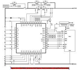
BQ76942 - Common Drain
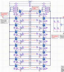
Our common source design.
We will drive the fets with an isolated gate driver that has a supply referenced to this common source. And driving logic signals will be coming from BQ76942. So there is no problem with using CHG and DSG pins of BQ76942.
But PCHG and PDSG pins creates some issues with common source config. I believe in order to drive the precharge FET given in figure 16-1 PCHG pin pulls the gate of precharge FET 8.4V below of PACK and to drive the predischarge FET given in figure 16-1 PDSG pin pulls the gate of precharge FET 8.4V below of BAT. Therefore creating the negative voltage needed to drive p channel fets.
Since I'm using a common source config. I can not connect this pins straight to my isolated gate driver input and expect it work. So I need to design a logic circuit that would change the PCHG and PDSG outputs into gate driver input logic signals. I think need to design the circuit referenced to PACK and BAT pins but I'm not really sure.
Am I on the right track?
Has anyone designed this kind of circuit?
Any tips on how to approach this problem?
Thanks in advance. Best regards,
