A related question is a question created from another question. When the related question is created, it will be automatically linked to the original question.
If you have a related question, please click the "Ask a related question" button in the top right corner. The newly created question will be automatically linked to this question.
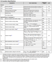
The insulation specifications found under 5.6 Insulation Specifications in the product's datasheet will be the right reference to use when analyzing the insulation.
As long as these specifications along with other ratings and recommendations in the datasheet such as the layout are followed, there should not be a risk for breakdown of the insulation barrier.
If there are any specific questions regarding these, please feel free to let me know.
In regards to the AMC1311BQDWVRQ1 part, please post a separate thread with this device tagged to receive support from the dedicated expert for this device.
We have confirmed from the datasheet that the device is specified as providingbasic insulation. However, we were unable to determine from the datasheet whether the internal insulation barrier of this driver is constructed asdouble-layeredor not. Could you please clarify this point?
Additionally, we are concerned about potential failures caused byPCB layout around the ICandmechanical stress on the board, which are not explicitly described in the datasheet. Could you advise on what kinds of failure mechanisms or design considerations should be taken into account in these areas?
We appreciate your guidance and look forward to your response.
Thank you very much for your response. I now understand that the UCC21330-Q1 provides single-level insulation.
In my application, insulation breakdown would constitute a hazardous event, so it is essential to clearly indicate the countermeasures implemented to prevent such occurrences.
To that end, I would like to ask for some additional clarification:
I understand that adhering to the specifications in the datasheet is key to preventing insulation breakdown. However, I would like to confirm which factors are particularly influential in causing such failures.
I believe that voltage stress and ESD applied to the input and output pins are relevant concerns. Would you agree with this assessment?
Alternatively, is the most critical factor the application of overvoltage between the isolated pins?
I appreciate your guidance and look forward to your response.
I understand that adhering to the specifications in the datasheet is key to preventing insulation breakdown. However, I would like to confirm which factors are particularly influential in causing such failures.
Outside of the datasheet specifications, the most important factor for preventing insulation breakdown would be the layout. However, designing around the layout recommendations will help prevent this from occurring. Recommendations such as avoiding traces/routing below the device, maintaining creepage between the primary and secondary sides as well as between channel A and channel B, will help.