This thread has been locked.

If you have a related question, please click the "Ask a related question" button in the top right corner. The newly created question will be automatically linked to this question.

TPSI31P1-Q1: Design-in questions

Part Number: TPSI31P1-Q1

Tool/software:

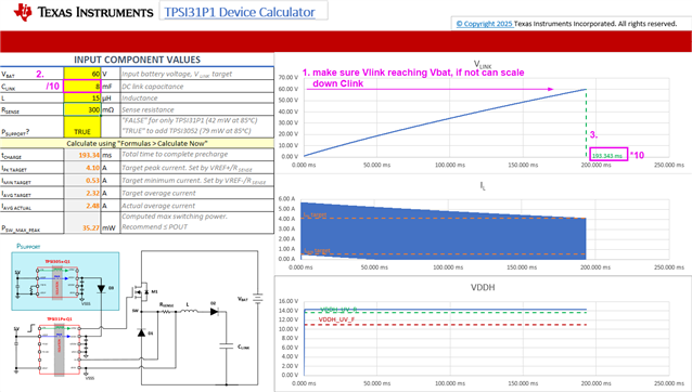
Hi, a few questions from the implementation point (this is for a lower voltage, 60V max system with about 40-80mF of capacitance)

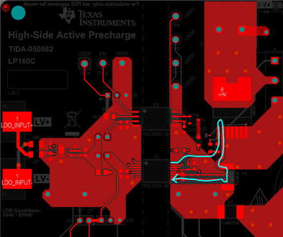
  1. What is the function of a safety cap/resistor network across the output that's present in the EVM design? Is that normally present in a production design?
  2. Any specific requirements for the diode D1 besides voltage/current? Does it have to be an Ultra fast recovery type?
  3. Same question for selecting the main FET- any specifics?
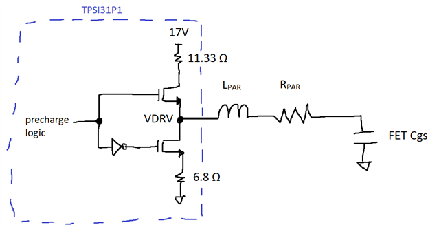
  4. The datasheet mentions a FET M2 to prevent reverse current flow, while the dev board goes with a diode- what is the rational there?

Thank you!

  • Hello Igor,

    Thanks for reaching out to our team on E2E.

    1. Capacitor and resistor string should be across the input. The capacitor helps stabilize the voltage seen at the input as there are fluctuations which can disrupt precharge. The resistors help ensure the capacitor discharges in case of failure where the precharge path fails open.
    2. Voltage and current are the main requirements for diode selection. I had originally selected ultra-fast in order to minimize reverse recovery variable, but I am not sure it really matters in this application.
    3. It is best select MOSFET with minimum gate charge (Qg) in order to maximize the driver's power for switching which in turn allows for smaller inductance. You can play with calculator tool values to see this effect.
    4. Either MOSFET or diode will work for blocking reverse current once the precharge circuit is off. I think for datasheet, sometimes we saw that SiC MOSFETs were cheaper than SiC diodes so included that in the diagram instead.

    Best regards, 
    Tilden Chen


    Solid State Relays | Applications Engineer

  • Thank you, that's very helpful. 
    Can we run our schematic by you via some type of PM once it's done?

  • Hello Igor,

    Thank you for your reply.

    Would be happy to support a schematic review once it is available, please DM me or send an email. I will DM my email to you.

    Best regards, 
    Tilden Chen


    Solid State Relays | Applications Engineer

  • Hello Igor,

    Just noticed your capacitance is large. If you are using the calculator tool and noticing the calculator is not displaying Vlink reaching Vbat, this is because the calculator is at max cell calculation capacity. To get around this, you can scale down Clink and multiply the final charge time by the scale. Image below to show what I mean, example for 80 mF capacitance, we can scale it down to 8 mF then multiply the final charge time by 10.

    Best regards, 
    Tilden Chen


    Solid State Relays | Applications Engineer

  • Thank you. We have not seen it fail to reach the VBAT but this makes sense.
    One question that did come up is FET selection if using standard NMOS FET. With the VDRV pin possibly reaching 17-18V it gets pretty close to a typical 20V VGS max. Should we be adding series resistance + clamp at the gate to avoid possibly damaging the FET?

  • Hello Igor,

    Thanks for your reply. I think the FET gate is safe from voltage spikes because of the internal Cgs and Cgd capacitances that "gradually" charge up or discharge during turn-on/turn-off like RC behavior. If we are expecting voltage spikes due to VL = L di/dt and parasitic inductance, since LPAR is small and di is small towards the end of RC charge/discharge, I do not think clamp is necessary.

    If we use VL = L di/dt, assume worst case with 2V spike, 10 mA over 1 ns, and solve for LPAR, LPAR = 20 µH which seems quite large.

    Best regards, 
    Tilden Chen


    Solid State Relays | Applications Engineer

  • To follow up on this- looking over the layout of the demo board vs the datasheet, the grounds are basically cleared from under the FET/Diodes/Inductors and only present under the IC. It is not clear to me how the IC connection to VSS is done- is it only via a sense line or is there a plane connection somewhere too?
    The datasheet indicates two places- the sense line but also the main ground separately connecting near the IC. On the EVK it's hard to tells from pdf pictures and the dev board but it seems the VSS on the chip is separated from the VSS plane near/under it? I see discrete traces connecting VSS pins with no planes around vias connecting them. 

  • Hello Igor,

    For ground, I was trying force the IC to reference the same point to avoid inaccurate current sense in the shunt especially during precharge when there is current flowing through. Image below to help explain. So there are ground (VSSS) planes but also a cutout around VSSS vias near IC on other layers to force the reference to the same node (bottom of shunt resistor).

    Best regards, 
    Tilden Chen


    Solid State Relays | Applications Engineer

  • So is U1 here only getting VSSS through that one bottom trace from pin 2 of Rsense? That would mean the returning gate drive current would go through that as a well?

  • Yes, gate drive current follows this path:

  • Thanks again, I'll send you our layout for review