Other Parts Discussed in Thread: TPS65987,
Tool/software:
Hi,
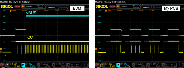
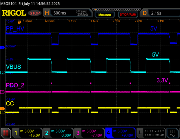
I made another PCB based on your EVM circuit (USB-C-PD-DUO-EVM).I am currently trying to connect the PCB I designed to the FTDI interface on your EVM and use the tps6598x application customization tool to burn the software into the TPS65987D on my PCB.
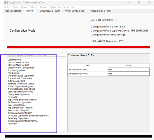
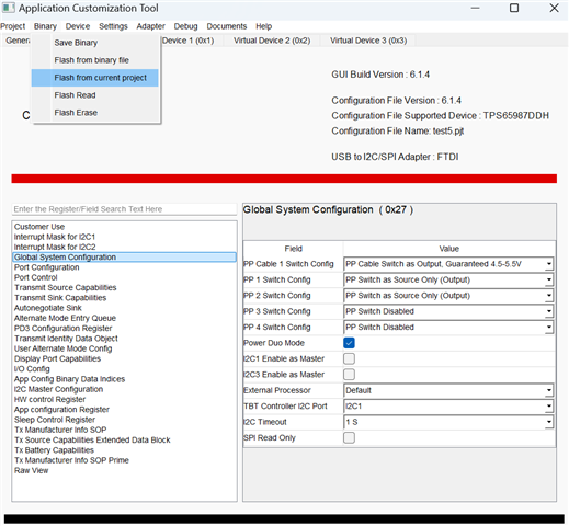
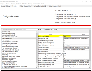
But currently I encounter the problem that SPI cannot read region, as shown below:
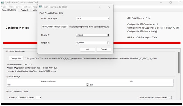
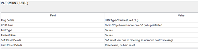
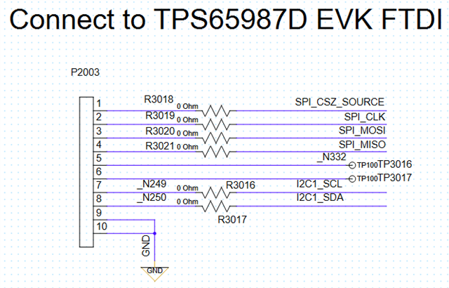
From what I understand, there is a SPI CS Header (J202) on the EVM. By shorting one end, the CS pin of the FTDI can be connected to the CS pin of the Source or Sink SPI Flash(U6 or U201) on the EVM, and then we can read its region through the tool. So I thought that if I connected the J2 Header on the EVM to the SPI Flash on the PCB I designed and J202 of EVM was not shorted at either end, the FTDI on the EVM should recognize the TPS65987D on my PCB and be able to read or burn it through the tool, but it doesn't seem to work. I'm not sure where I went wrong.
Does the TPS65987D need to be pre-programmed before it can be read SPI region via FTDI with the application tool, or does the SPI Flash have any specification requirements?
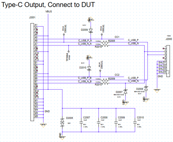
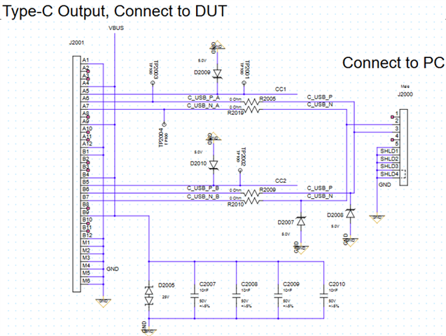
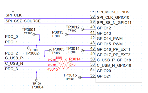
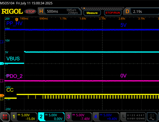
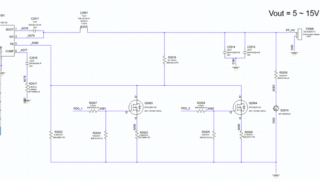
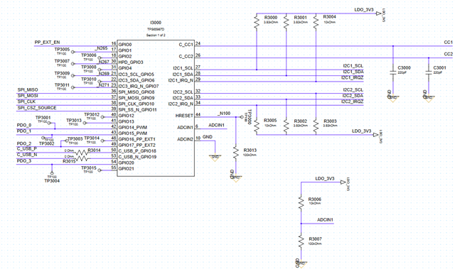
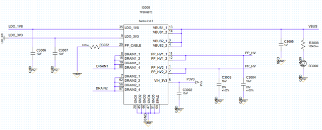
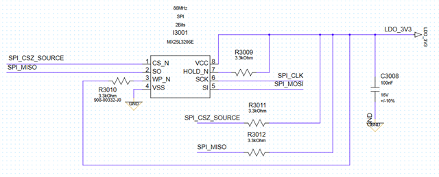
Below is my circuit:
- TPS65987D
- SPI Flash
- SPI/I2C Header
Basically, the design is similar to the source PD controller on the EVM, but some parts have been simplified and some components are selected with different specifications but similar functions, and P3V3 is powered by an external power supply.