This thread has been locked.

If you have a related question, please click the "Ask a related question" button in the top right corner. The newly created question will be automatically linked to this question.

TPS7A45: TPS7A4501

Part Number: TPS7A45

Tool/software:

Hello,

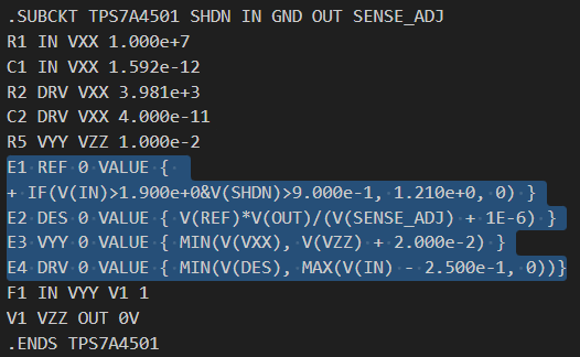
Could you help me please with an LTSpice simulation model for TPS7A45xx?

I tried to use the one that you provide but it doesn't work.

Thank you,

Marius


  • Hi Marius,

    It appears that the PSPICE transient model is encrypted and will not work outside that software. Unlike many of our other chips, we have not released a fully unencrypted PSPICE model for this part. The TINA model .lib file, however, is not encrypted but also not in the LTSPICE format. You could likely make it work by manually converting the 4 voltage dependent voltage sources from the TINA syntax to the LTSpice syntax:

    LTSPICE: https://ltwiki.org/LTspiceHelp/LTspiceHelp/E_Voltage_Dependent_Voltage_Source.htm

    Essentially: I would try changing VALUE {<expression>} to value={<expression>} and try importing that modified netlist

    What issue are you facing with using the TPS7A45? 

    Thanks,

    Gregory Thompson

  • Hello,

    Thank you very much for your feedback. I will try to convert E1 to E4 to LTSpice syntax, even if I am not very good in LTSpice.

    I am just performing an analysis of the supply circuit due to some transients that could be on the input supply.

    The Vin of TPS7A4501 is 15V and the output is adjusted to 12V, by using a 29K4 and a 3K3 resistors.

    It is known that the LDO is working as a step down converter, and the input voltage shall be higher than the output voltage + the voltage drop across the LDO.

    Due to these transients that could be on the input supply the 15V input can decrease below the 12V output, so I want to see if the TPS7A45 will still work, or will it shut-down when the input voltage is below the set output voltage?

    Best regards,

    Marius

  • Hello Gregory,

    I see that the lib file contains few resistors and capacitors that are connected between different nodes such as IN, VXX, DRV, VYY.

    First of all, could you tell me please what is the purpose of those resistors and capacitors, because I didn't find them in the datasheet.

    Secondly, could you tell me please the meaning of VXX, VYY, VZZ, DRV, and DES nodes?

    Thank you,

    Marius

  • Hi Marius,

    It's quite an old and idealized model that should simulate the part's basic properties but won't necessarily reflex the real internal structure. Many things are added as extreme values to ensure convergence and efficiency.

    Though this model was made before my time, a basic rundown on it's structure:

    The resistors and capacitors don't correspond to anything physical or that you'd find in the datasheet but are part of the way the device is modeled. R1,R2,C1,C2 form a resistor divider a smooth resistor divider between IN and DRV and are given quite extreme values to minimize their impact on the rest of the circuit. R5 is part of the way it outputs voltage. VXX VYY and VZZ are arbitrary internal nodes. VXX is the output of the voltage divider, VYY and VXX are part of the way it outputs voltage. DES is the output of the feedback function, DRV is basically the output of buffer from DES the with some limit behavior for what I believe is dropout. 

    Best,
    Gregory Thompson