This thread has been locked.

If you have a related question, please click the "Ask a related question" button in the top right corner. The newly created question will be automatically linked to this question.

TPS53015: TPS53015 output not getting 5V , instead getting the 0.8V

Part Number: TPS53015

Tool/software:

Hi Team,

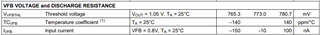
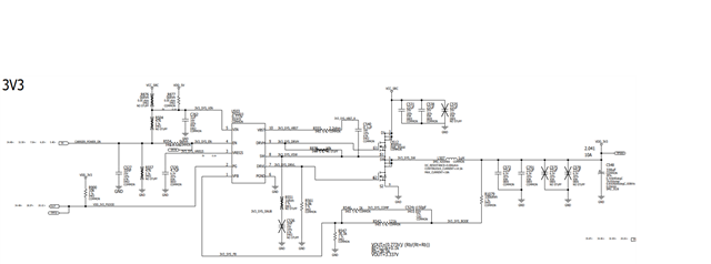
As we are using the module TPS53015 as in our design for the application of 12V to 5V, we are not getting Expected output voltage as 5v, in this query i am sharing the Schematics we have used to get the 5V from the 12V

input.

In the schematics, VCC_SRC_FET is 12V, 

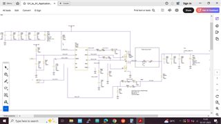
please let us know, is there any wrong with the design 

  • Any help on this

    thanks

    SAI KIRAN 

  • Hi Sai Kiran

    TI USA is on holiday from July 4th to July 6th.

    Can you provide, Vin, EN, SW, Vout wave forms during operation where you see vout and no vout

    Thank you

    Savith

  • Hello Savith Kumar,

    Thanks for your response,

    please find the attached pdf for the waveforms, 

    TPS53015_waveforms.pdf

  • Hi Sai Kiran,

    Savith will respond this week

    Thanks,

    Calan

  • Hi Calan Elaya,

    Thanks for the update

    thanks,

    SAI KIRAN

  • Hi,

    any update on this?

    i have doubt with Switching frequency of IC, actually the datasheet is telling 500kHz, but on the CRO i am saw only 160kHz switching, please verify with the above uploaded pdf TPS53015_waveforms.pdf

    thanks,

  • Hi Sai Kiran

    Looking at the SW node wave forms it is in DCM where load current < Iripple/2  and also can you look at the FB to GND wave form , is this regulating at at required FB voltage of 0.773V

    and also try reducing the Cff to 15pF and see if part comes back to regulation

    Thank you

    Savith

  • Hi Savith Kumar,

    I tested the voltage between FB and GND, and it is reading 0.839V. and output voltage at C551 is 0.815V

    i removed Cff i.e C791 i have  tested ouput volatge which is redaing 0V. is really required C791.  what will happen if we replace 150pf to 15pf.

    thanks,

    SAI KIRAN

  • Hi Savith Kumar,

    I tested the voltage between FB and GND, and it is reading 0.839V. and output voltage at C551 is 0.815V

    i removed Cff i.e C791 i have  tested ouput volatge which is redaing 0V. is really required C791.  what will happen if we replace 150pf to 15pf.

    and i have changed C791 to 10pF and tested. still output voltage is 0.8V

    I tested the voltage between FB and GND, and I observed some strange behavior at the output.

    Immediately after powering ON, the voltage at C551 (output capacitor) is around 0.8V.

    However, when I probe the voltage at FB and GND using the DMM, within a fraction of a second the DMM initially shows 0.9V, and then it suddenly drops to 0V.

    After that, when I check the voltage at C551 again, it also reads 0V, even though it was 0.8V earlier. FB pin is loaded by DMM?

    How to solve this issues?

    thanks,

    SAI KIRAN

  • Hi Sai Kiran

    DMM have high impedance and not likely loading the FB

    Pls share the Layout. is there any other leakage path for Vout and FB on the board?

    Vref in you measurements show higher value than the datasheet spec

    can you replace the IC with working TPS53015 or a new IC to see if it is related to layout 

    here are some app notes to understand the Feed forward capacitor effect

    www.ti.com/.../slva289b.pdf

    www.ti.com/.../slva466a.pdf

    Thank you

    Savith

  • Hi,

    Vref in you measurements show higher value than the datasheet spec --  i also wondering why,

    please find the layout,

    can you replace the IC with working TPS53015 or a new IC to see if it is related to layout      ---- I have replaced with new IC, but still same response getting 0.8V from at Vout.

    Have you reviewed the Switching frequency from the above waveform, which we have forwarded earlier.  i saw switching frequency as 160Khz on CRO , from data sheet it is 500Khz.

    thanks,

    SAI KIRAN

  • Hi Sai Kiran

    will get back to you in couple of days

    Thank you

    Savith

  • Hi Savith Kumar

    please help us in this,

    we need to dispatch the unit, Because of this module not giving the output it is getting delay.

    hope you will understand our situation.

    thanks,

    SAI KIRAN

  • Hi Sai Kiran


    1. the frequency you are seeing is lower because device is operating in Auto skip (DCM) mode as I mentioned earlier when the load < inductor current ripple/2.

    2. the Feed back is greater than the Vout suggests that something is pulling on the feed back, it can either be solder, short, layout issues, wrong or damaged component on the feed back circuit , the layout image you sent does not tell anything that is wrong, SW node is as expected.

    3. pls measure the component values in feed back circuit and verify they are correct

    4. provide Vout, VFB , SW wave forms with 1us and 2us time scale

    Thank you

    Savith

  • Hi Savith,

    I had measured the components values in the feedback circuit. Everything as expected.

    R966 is 121K, R967 is 1K, C791 as per your suggestion i have changed to 10pF, but when measuring R975, i should get 22.1K but getting nearly 2.3K, even i have changed with new 22.1K resistor, when i am measuring across it with DMM again it is showing 2.3K only.  may IC internal circuit parallel to it?

    As you asked for waveforms,

    actually, we are making two prototype boards. previously shared waveforms from the first board, now i am sharing second boards.

    here Vout is same getting 0.8V but MOSFETs switching also not happening i guess, but Vreg and enable is okay. kindly please check the below pdf.

    TPS53015_waveform_Second_board.pdf

    thanks,

    SAI KIRAN

  • Hi Sai Kiran

    apologies I should have been more clear when I asked Vout and FB waveforms it is the ripple wave form that I am asking 

    can you provide the ripple waveform for both VOUT and FB 

    did you also measure the value of R975 by removing from the board

    Thank you

    Savith

  • Hi Savith,

    I understood what you’re asking regarding the waveforms. The latest waveforms I shared are from the second board, which is a copy of the first board. However, the behavior of this board seems different — there are no MOSFET gate drive signals from the IC (DHRH and DHRL), as shown in the waveforms.

    Despite that, the Vout is the same as the first board — 0.8V.

    Regarding your request for Vout and FB ripple waveforms — should I capture them in AC coupling mode? Please confirm how exactly you'd like them to be captured.

    for your information, we are using TPS53015 IC design in the NVIDA jetson AGX Orin carrier board. 

    thanks,

    SAI KIRAN

  •    

      will be out of the office for a few days, so I will be stepping in to help.

    There are several indications from what you have provided that some external circuit, PCB or assembly issue is pulling up on the output voltage or feedback path, and that is the route cause of the issue.  This includes the VFB pin being higher voltage than the output, and the VFB voltage not aligning VOUT x (R975 / (R975 + R966) ), and also VOUT being 0.8V with no activity on the switching node or gate drive voltages.

    The TPS53015 controller is not designed to sink current from VOUT.  It it designed to use the external MOSFETs to drive a VOUT voltage to maintain 0.773V at the FB voltage.  It does this by turning the high-side MOSFET (Q1) on when it detects VFB less than 0.773V, then turning Q1 off and turning the low-side MSOFET (Q2) on after a fixed on-time.  Q2 then stays on until the current in Q2 is detected to reach 0A, as sensed by the SW pin rising to 0V, or the VFB voltage drops back to 0.773.

    If something is externally pulling VFB above 0.773V, the MOSFETS stay off and the output does not switch.

    Regarding your request for Vout and FB ripple waveforms — should I capture them in AC coupling mode? Please confirm how exactly you'd like them to be captured.

    We are looking for the shape and timing of the VFB and VOUT waveforms, so it would be best to keep them DC coupled so we can see the VFB = 0.773V level.  We would like to see them at 1μs per division, 10μs per division, and, if they are oscillating, at a time division that shows a few cycles of the oscillation.

    Ideally, we would like to see both VOUT and VFB voltage on the same oscilloscope image.

    Can you disable the TPS53015 by shorting R335 (EN to GND) to turn the output off and measure VFB and VOUT?

  • Hi Peter James Miller,

    I'm glad to hear that you're willing to help me resolve this issue.

    As per your request, I have captured the signals at both 10 µs and 1 µs time bases.

    Please find the attached PDFs for your review.

    Thank you,
    SAI KIRANTPS_waveforms_with_1us_timeScale_with_enble.pdfTPS53015_waveform_10us_timeScale_with_enable.pdfTPS53015_waveforms_Time Scale_1us_and_10us_without_enble_supply.pdf

  •   

    The average voltage for VOUT, and VFB are different for your different measurements.

    In the first figure for the 1μs time scale, VOUT is 835mV, in the third figure, it's 946mV

    In the second figure, VFB is 904mV, the third it's 958mV. 

    We see something similar, but to a lessor extent in the 10μs scale.  I have to conclude that there is a large (>100mV) AC ripple on VOUT and VFB that is much lower than 10kHz.  The HDRH / SW waveforms at 10μs show the switch-node frequency is also much lower than 10kHz.

    To confirm that, please set up the scope in the following setting:

    Channel 1:

    Connect to SW

    Vertical resolution 10V/Division

    Vertical Position: 0V set to -3.5 divisions (0.5 divisions up from the bottom of the screen)

    Channel 2:

    Connect to VFB

    Vertical Resolution: 200mV/Division

    Vertical Position: -2 divisions (2 divisions up from the bottom of the screen.  This will allow upto +6 divisions on the screen, for 0 to 1.2V) 

    Trigger

    Trigger on rising edge of Channel 1 (SW) at 6.0V level (VIN/2) 

    Trigger Position: Set to middle of screen

    Horizonal 

    Start at 10μs / division

    Increase time / division (50μs, 100μs) etc until at least 3 SW pulses appear on the display.

    I am expecting that we will see VFB discharging down to 773mV, then triggering an SW pulse, charging up, and then discharging back down to 773mV.  That would indicate that the TPS53015 is working correctly.

    Since we are not seeing the expected VFB / VOUT ratio set by the R966 and R975 divider, we need to conclude that something is in error with the divider.

    R966 is 121K, R967 is 1K, C791 as per your suggestion i have changed to 10pF, but when measuring R975, i should get 22.1K but getting nearly 2.3K, even i have changed with new 22.1K resistor, when i am measuring across it with DMM again it is showing 2.3K only.  may IC internal circuit parallel to it?

    Then the board is not powered, the VFB pin should not be leaking enough current to measure 2.3k from VFB to GND, but if the VFB to GND resistance was really 2.3k instead of 22.1k, the output voltage would be higher, not lower, and we should see a larger VFB to VOUT ratio, so I don't think that is the problem.

    Check the GND connection R975 to make sure it has a good solder connection and good connection to ground.  If R975 is not connected to GND, that would create the issue we are seeing.

    Use a DMM or Ohmeter to measure the resistance from the GND terminal of R975 to another ground point on the board in order to verify that R975 is connected to ground.   The resistance should measure under 1Ω

    Check the VFB connection of R975 to make sure it has a good solder connection.

    Use a DMM or Ohmeer to measure the resistance from the VFB terminal of R966 to the other ground point on the board.  This will confirm the resistance of R975 and it's connection to VFB.  The resistance should measure 22.1k (or at least, it should be the same as measuring across R975) this will check the connection from VFB to R975 and the connection from R975 to GND.

    There might be a bad solder joint on R975, or a bad ground via from R975 to ground.

  • Hi,

    I will share the CRO outputs by tomorrow, as I currently do not have access to them.

    In the meantime, I have performed some resistance measurements using a DMM:

    • R975 GND Check: I measured the resistance from the GND terminal of R975 to another known ground point on the board. It shows 0.7Ω, which confirms that R975 is properly connected to ground.

    • R966 VFB Path Check: I measured the resistance from the VFB terminal of R966 to the same ground point. It reads 2.3kΩ.

    Due to this reading, I suspected the value might be off, so I replaced R975 with the actual 22.2kΩ resistor. However, after mounting, it still shows 2.3kΩ, which is unexpected.

    Please let me know your thoughts or if you'd like me to check anything else.

    Thanks,
    Sai Kiran

  • I agree, that is unexpected. but suggests that there may be something else connected to the VFB net that might be sourcing current into VFB.

    Can you try removing R975 and measure the resistance from VFB to GND?

    You should also be able to turn the converter on with R975 removed, though the expected ouptut voltage would be .773V with R975 removed.

  • Hello,

    I have removed and tested, Gettting Vout as 0.773 and VFB is 0.812V

    thanks,

    SAI KIRAN

  •    

    I have removed and tested, Gettting Vout as 0.773 and VFB is 0.812V

    Thank you.  That still leaves us with the conclusion that something other than VOUT is sourcing current into the VFB node.  The Oscilloscope waveforms I asked for back on July 17th would help determine likely causes, but in addition to taking the oscilloscope waveforms, I would recommend checking the actual board for solder shorts or other connections from VFB to something else that might be pulling it up separate from VOUT. 

  • i will checked the soldering on the PCB, is fine.

    i want to share you one thing here, we have used TPS53015 in same PCB for the 3.3V output application. that is working fine. 

    this circuit is giving 3.3V output. 

    placement wise and soldering is same for the board circuits.

    FYI, our board is custom carrier board for NVIDIA jetson AGX orin SOM.

    thanks,

    SAI KIRAN

  •   

    Can you try swapping the TPS53015 controllers between the two locations to see if the issue follows the device or the application location?

    Have you made any progress on capturing the waveforms that I asked for? 

    To confirm that, please set up the scope in the following setting:

    Channel 1:

    Connect to SW

    Vertical resolution 10V/Division

    Vertical Position: 0V set to -3.5 divisions (0.5 divisions up from the bottom of the screen)

    Channel 2:

    Connect to VFB

    Vertical Resolution: 200mV/Division

    Vertical Position: -2 divisions (2 divisions up from the bottom of the screen.  This will allow upto +6 divisions on the screen, for 0 to 1.2V) 

    Trigger

    Trigger on rising edge of Channel 1 (SW) at 6.0V level (VIN/2) 

    Trigger Position: Set to middle of screen

    Horizonal 

    Start at 10μs / division

    Increase time / division (50μs, 100μs) etc until at least 3 SW pulses appear on the display.