This thread has been locked.

If you have a related question, please click the "Ask a related question" button in the top right corner. The newly created question will be automatically linked to this question.

TPS55340: Boost Converter SW Node Ringing

Part Number: TPS55340

Tool/software:

Hello,

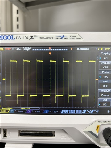
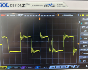
My TPS55340 boost converter's SW node is ringing quite a bit, contributing to audible noise and EMI.

12 V in, 24 V out, 0.5 A out

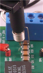
Here is the layout and schematic:

Inductor is FXC0630-100M.

Any recommended courses of action? Thanks!

  • Hi Desmond,

    Please follow below items when performing the measurement:

    • Make sure you are measuring with a ground springing.


    • Use high sample rate (<1ns/pt) and >200MHz bandwidth
    • Use scope full Y-axis scale

    The switching node waveform is not stable. That means you may have a bad loop.

    Please check the loop compensation with SLVC430  TPS55340 Boost Design Excel Spreadsheet Tool.

    Best Regards,
    Feng

  • Thanks for the reply. I was indeed using ground spring for scope measurement.

    Here is Bode plot from the current components (Rcomp = 10.7k, Ccomp = 33n, Chf = 47p, Cff = 120p):

    And after tweaking the values using the application schematic from the datasheet (Fig. 8-1) (Rcomp = 2.55k, Ccomp = 150n, Chf = 150p, Cff = 120p):

    Looking at total phase/gain, it looks more stable, as before 0dB gain occured near the knee of the phase plot. Lowering Rcomp seems to improve things even more. Is this sufficient? 

    Thanks

  • Hi Desmond,

    Both bode plot looks good. Can you share the design calculator? 

    Is the audible noise gone with the new compensation?

    Best Regards,

    Feng

  • Hi, I haven't had a chance to solder on a new compensation network as I do not have the components for it yet.

    Here is the Excel calculator: TPS55340 Parameter Calculation.xls

    Is there too much parasitic inductance in the layout, or perhaps not enough output capacitance?

    Thanks

  • Hi Desmond,

    The loop looks good. However, it may not be real.

    Please check the DC bias derating of the output ceramic capacitors as a first step.

    Best Regards,
    Feng

  • Hello,

    The voltage rating for the 3x 22uF output capacitors is 35 V. However I will try adding an external capacitor.

    Thanks

  • Hello, I added a 330 uF electrolytic to the output, and although the audible noise reduced considerably, the ringing on the SW node is still present.

  • Hi, it was indeed the compensation loop. I had an 0402 1kΩ resistor on hand and replaced the 10.7k Rcomp resistor with 1k; ringing went away on SW node, no audible noise, output ripple went from 3-5% down to <1%, and efficiency climbed from 84% to 92%. Here is the SW node now, under full load: