This thread has been locked.

If you have a related question, please click the "Ask a related question" button in the top right corner. The newly created question will be automatically linked to this question.

TPSM33625: Device damage after 20s of operation

Part Number: TPSM33625

Tool/software:

Hello,

We used the part in our design as a regulator from  +24V input to +5V. When powered up for the first time with +24V applied and minimal load (around 50mA), it regulates to the intended voltage by around 20 seconds and then the input current rises, it stops to regulate the output and heat up dramatically. After that the device is permanently damaged and it does not return to the initial behavior if power off and on. We found out that if the input voltage is smaller than 15V, the catastrophic failure does not happen, at least in the observed time. 

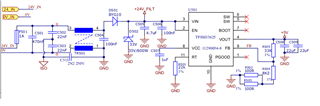
Please find the schematics below. We checked against the datasheet and could not find any discrepancies. The fact that it does work as intended for a small amount of time seems to be an indication that the general connections are ok. Also, we could not figure out what could cause such a catastrophic failure. 

We also experimented increasing the input capacitance with a low ESR capacitor, to no effect. In one test, we applied the input directly to +24_FILT node, with the same outcome.

Do you have any suggestions of how to proceed? What could cause such catastrophic failure in this part?  Is there any know history of counterfeits for this part that could explain this issue?

Thanks in advance

  • Hi,

    If you are utilizing an input filter, it is important to ensure that the input filter is effectively damped (with an electrolytic capacitor with enough ESR), to avoid any runaway inductive ringing on input. Please see this application note for details on a damping capacitor (Cd in the application note).

    If this does not help, please send over the layout used so we may review this as well.

    Thank you,

    Joshua Austria

  • Thank you for the reply. 

    We tested applying the input voltage with a lab power supply directly in the +24V_FILT node without the diodes, with the same result.

    Please find below the layout. It was done in a hurry, so some aspects of it are not ideal, but we can't figure out what could cause such catastrophic failure. Would you know of any cases of counterfeits for this part?

  • Hi Marcelo,

    Applying the input voltage directly at the 24V_FILT node can still be subject to extra inductance. Please see section 8.4 of the datasheet that delves into more detail about this.

    In terms of the layout, I have a couple of notes:

    • The input trace from the VIN pin to the input capacitors is very long and narrow. This adds extra impedance and is not recommended for this design. It is important to keep these capacitors as close to the VIN pin and ground pins as possible to keep the high di/dt trace from emanating too much noise. This also plays into the aforementioned undamped input.
    • The ground plane overall is very thin and unoptimized for both noise reduction and thermal dissipation.Generally a 4 layer board is recommended for this device to aid in heat dissipation and to help with signal routing.
    • The feedback resistors are located directly besides the SW node. The SW node is the noisiest aspect of the device and can corrupt the sensitive feedback pin and thus the regulation of the device. It is recommended to keep the feedback network as a whole away from the SW node.
    • For more information about a recommended layout, please see section 8.5.2 of the datasheet for a layout example and section 8.5 of the datasheet for overall layout guidelines.

    Thank you,

    Joshua Austria

  • Thank you for the observations.

    When we tested your suggestion in relation to runaway inductive ringing on input generated by the input filter we removed all circuitry related to the filter and placed a large very low ESR electrolytic capacitor in the input pins. The additional capacitor and the input voltage were applied very near the VIN. Please elaborate on how to properly perform this test to confirm this as a cause. We also probed the input and output and found no oscillation or spikes. The operation seems stable until 16V input.

    Regarding the layout notes, would you know how any of these items could cause the catastrophic failure observed? We did not observe any heat issues during the operation at lower voltages where it does regulate, and noise coupling in the feedback pins should interfere with the regulated voltage, or even make it not regulate properly, but not burn the device right?

    Any suggestions on how to narrow down what can be the cause? We cannot perform a layout revision without pinpointing the exact issue for the failure. 

    Also, do you know of any cases of counterfeits for this part?

  • Hi Marcelo,

    I am not sure what I can comment on in regards to counterfeits for this part, but this is always a possibility. If you are worried about counterfeits, please share a picture of the device and a description of how the device was obtained. You can also order this device directly from TI.com and see if there is any difference in its behavior when compared to your suspected parts.

    In regards to the layout recommendations I gave, each one of the items I presented could result in a failure. I would be hesitant to dismiss any of the recommendations as these are datasheet guidelines provided for the part. In my experience, deviating from the datasheet layout recommendations often results in catastrophic failure.

    As for the input voltage trace, the best practice is to place your ceramics the closest to the input and ground pins, whereas the electrolytic can be placed somewhat far. The important aspect of the electrolytic capacitor is its ESR, and you want this value to be sufficient to damp any inductive ringing that can come from your input lines/testing environment. The best way I have found to test this is to probe the input pin of the device itself and compare it to the input voltage waveform that is being applied to your board. Without the sufficient electrolytic ESR, this inductive ring can be substantial. This ring will also get worse when a load is applied to the device's output.

    Thank you,

    Joshua Austria