A related question is a question created from another question. When the related question is created, it will be automatically linked to the original question.
If you have a related question, please click the "Ask a related question" button in the top right corner. The newly created question will be automatically linked to this question.
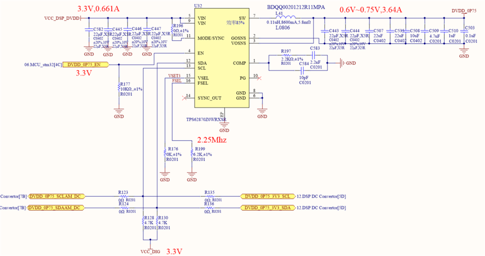
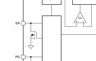
1. Please connect EN pin to a resistor at least 15k ohm.
2. Are there any load transient requirements to meet? Because the compensation circuit, R197 and C583, is heavily affected by the output capacitance and load transient requirements. Can you please check Vout tolerance specs and load step condition (Iout_min, Iout_max and slew rate) and provide me this information to help me check the compensation? You can also find the calculator here: TPSM8287A-COMPONENT-CALCULATOR Calculation tool | TI.com
Besides, can you pls share what is the load SoC here?
1.For the EN pin, can I connect a 15kΩ pull-down resistor to GND as shown in the schematic I provided earlier? Or does it need to use a series resistor instead?
2.The DSP datasheet does not mention any load transient requirements. The only related specification is that the power supply ramp step must not exceed 4mV/step.I also checked the DSP reference design, and it uses the same power IC with C583 = 2.2nF, C584 = 10pF, and R197 = 2.15kΩ, which is similar our current design.
The EN pin use a transistor inside, as we can see in the block diagram in the datasheet. Therefore we need a 15k ohm resistor to limit the current flowing into the pin when it's pulled high.
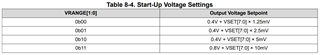
The Vout ramp step can be set through I2C as in the datasheet.
The chip can work with the previous compensation setting. But we need to pay attention that with that setting, the bandwidth is large and might make the system more sensitive. This is usually used to meet very strict load transient requirement. Therefore, it would be helpful if we can check it with the load transient requirement.