This thread has been locked.

If you have a related question, please click the "Ask a related question" button in the top right corner. The newly created question will be automatically linked to this question.

TPS54340B-Q1: More radiated emission

Part Number: TPS54340B-Q1

Tool/software:

Hello,

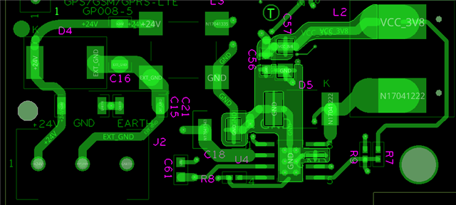
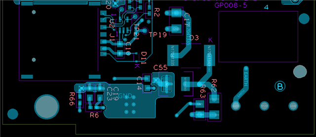
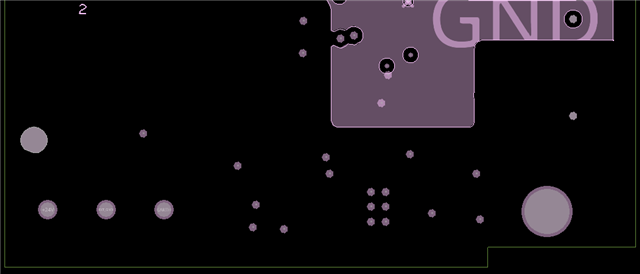
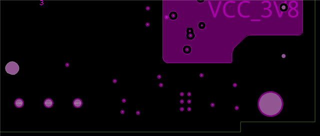
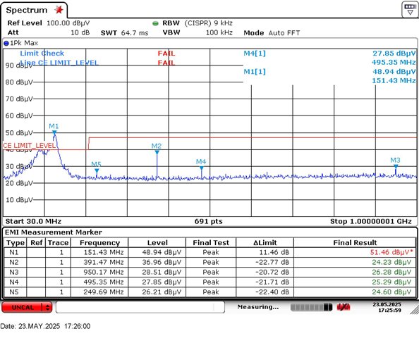
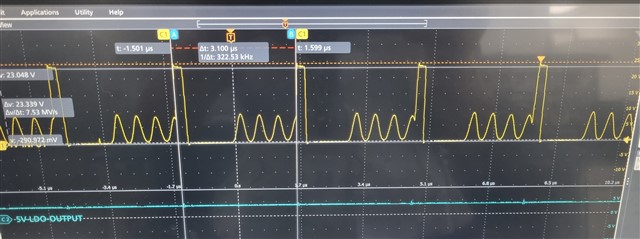
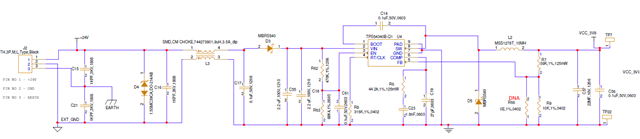
I am using TPS54340B-Q1 in my design. we are converting 24v to 3.8v using this IC. during radiation emission test we observed that we are getting more radiation from this IC. can you please support me how to reduce radiated emission from TPS54340B-Q1. Also please share how much this IC radiate. For reference circuit screen shot is added here.

Thanks

Meghna Khadikar

  • Hi Meghna,

    Can you please share your layout for this device as well? I can do a full design review to help with improving radiated EMI performance. 

    Can you also share what results you received from your radiated emission test?

    Thank you,

    Joshua Austria

  • Hi Joshua,

    Thanks for your reply. Please find details below:

    1. Board is 4 layer board

    Top Layer

    Bottom Layer

    GND Layer

    VCC Layer

    Image of Radiation

    Image of waveform on oscilloscope for SW node

    Thanks

    Meghna Khadikar

  • Hi Meghna,

    I reviewed both your schematic and layout and this is what I found:

    Schematic:

    • The component selections overall look ok. Please ensure that your inductor is rated at least as high as the high side switch current limit of the device to avoid hard saturation (5.5A).
    • A lower profile inductor will aid in radiated electromagnetic interference (EMI) performance
    • A damping capacitor on VIN can help with ensuring that the inductive ring from your input filter does not cause an out of spec operation on input.
    • A snubber on SW can be added to help curb radiated EMI. Please see this technical note for help in designing the snubber circuit appropriately: https://www.ti.com/document-viewer/lit/html/SSZTBC7 

    Layout:

    • Overall, it is recommended that each layer have a ground pour that covers all available space. Ground helps sink some high frequency noise and can shield some more sensitive traces/signals from the high di/dt loops that characterize buck converters.
    • The input capacitors need to be placed as close as possible to the VIN pin. The VIN capacitors are a major portion of the high di/dt loop from VIN to the FETs that will create noise. Any increase in inductance on this path will result in worse EMI performance.
    • It is also recommended that the boot capacitor be placed as close as possible to the boot pin.
    • It looks like there is a via on the SW node. Please note it is not recommended for the SW node to have any through hole connections as this will effectively spread the SW noise into the entire system. Keeping the SW node as small and isolated as possible is critical to ensuring good EMI performance.
    • Overall, please check section 10.2 of the datasheet for an example of a good layout with this IC.

    Thank you,

    Joshua Austria

  • Hello Joshua,

    Thanks for your reply. 

    I have one request could you please share radiation emission report of this IC. I would like to know in best condition what is the range of radiation emission of this IC.

    Thanks

    Meghna Khadikar

  • Hi Meghna,

    Unfortunately I do not believe we have a radiation emission report of this IC. 

    Thank you for understanding,

    Joshua Austria