This thread has been locked.

If you have a related question, please click the "Ask a related question" button in the top right corner. The newly created question will be automatically linked to this question.

BQ25756E: Charging current

Part Number: BQ25756E

Tool/software:

Hello, 
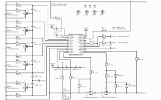
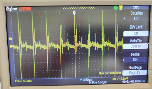
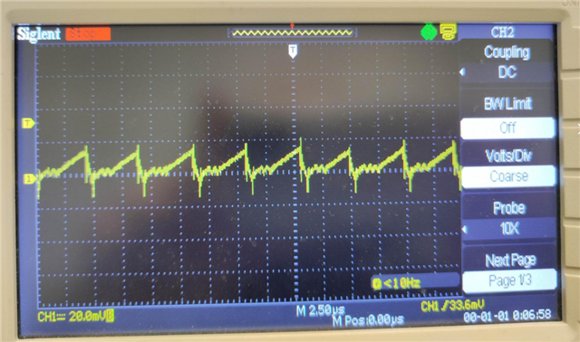
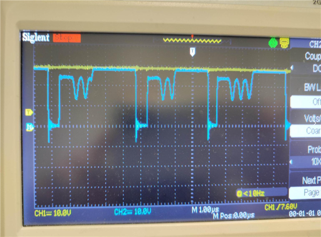
I have 5 cells in series using bq7791500 BMS I have tested separately that part with 2 A charging current and it works fine. 
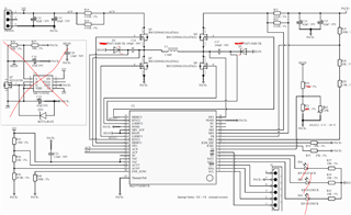
After connecting the charger i cant get more than 0.9A of charging current. 

Input voltage 24V 
Battery pack discharged to 18V

  • Hi,

    Kichg is 50 A * kOhm. On the ICHG pin, there is a 47 kOhm resistor. The charge current is limited to Kichg / ICHG -> 50 / 47 = 1.064. Does the circuit behavior improve when this resistance is decreased?

    Best regards,
    Michael

  • I've decreased it to 18kohm but there is no difference

  • Can you send a register reading of our I2C registers?

    Best,
    Michael

  • I cant read the registers all I get is FFFF on all registers. 
    I have pulled CE low and i am using mcu to read the registers. 

  • That register reading seems incorrect to me. Are you able to share the relevant code that reads the registers from the MCU?

  • /* USER CODE BEGIN Header */
    /**
      ******************************************************************************
      * @file           : main.c
      * @brief          : Main program body
      ******************************************************************************
      * @attention
      *
      * Copyright (c) 2025 STMicroelectronics.
      * All rights reserved.
      *
      * This software is licensed under terms that can be found in the LICENSE file
      * in the root directory of this software component.
      * If no LICENSE file comes with this software, it is provided AS-IS.
      *
      ******************************************************************************
      */
    /* USER CODE END Header */
    /* Includes ------------------------------------------------------------------*/
    #include "main.h"
    
    /* Private includes ----------------------------------------------------------*/
    /* USER CODE BEGIN Includes */
    #include <stdio.h>
    /* USER CODE END Includes */
    
    /* Private typedef -----------------------------------------------------------*/
    /* USER CODE BEGIN PTD */
    
    /* USER CODE END PTD */
    
    /* Private define ------------------------------------------------------------*/
    /* USER CODE BEGIN PD */
    //extern I2C_HandleTypeDef hi2c1;
    
    #define BQ25756E_I2C_ADDRESS    (0x6A << 1) // 7-bit address 0x6B, shifted for 8-bit R/W byte
    //extern I2C_HandleTypeDef hi2c1; // Assuming I2C1 is used
    I2C_HandleTypeDef hi2c1;
    /* USER CODE END PD */
    
    /* Private macro -------------------------------------------------------------*/
    /* USER CODE BEGIN PM */
    
    /* USER CODE END PM */
    
    /* Private variables ---------------------------------------------------------*/
    const uint8_t bq25756e_register_map[] = {
        0x00, // REG0x00_Charge_Voltage_Limit
        0x02, // REG0x02_Charge_Current_Limit
        0x04, // REG0x04_Input_Current_DPM_Limit
        0x06, // REG0x06_Input_Voltage_DPM_Limit
        0x0A, // REG0x0A_Reverse_Mode_Input_Current_Limit
        0x0C, // REG0x0C_Reverse_Mode_Input_Voltage_Limit
        0x10, // REG0x10_Precharge_Current_Limit
        0x12, // REG0x12_Termination_Current_Limit
        0x14, // REG0x14_Precharge_and_Termination_Control
        0x15, // REG0x15_Timer_Control
        0x16, // REG0x16_Three-Stage_Charge_Control
        0x17, // REG0x17_Charger_Control
        0x18, // REG0x18_Pin_Control
        0x19, // REG0x19_Power_Path_and_Reverse_Mode_Control
        0x1A, // REG0x1A_MPPT_Control
        0x1B, // REG0x1B_TS_Charging_Threshold_Control
        0x1C, // REG0x1C_TS_Charging_Region_Behavior_Control
        0x1D, // REG0x1D_TS_Reverse_Mode_Threshold_Control
        0x1E, // REG0x1E_Reverse_Undervoltage_Control
        0x1F, // REG0x1F_VAC_Max_Power_Point_Detect
        0x21, // REG0x21_Charger_Status_1
        0x22, // REG0x22_Charger_Status_2
        0x23, // REG0x23_Charger_Status_3
        0x24, // REG0x24_Fault_Status
        0x25, // REG0x25_Charger_Flag_1
        0x26, // REG0x26_Charger_Flag_2
        0x27, // REG0x27_Fault_Flag
        0x28, // REG0x28_Charger_Mask_1
        0x29, // REG0x29_Charger_Mask_2
        0x2A, // REG0x2A_Fault_Mask
        0x2B, // REG0x2B_ADC_Control
        0x2C, // REG0x2C_ADC_Channel_Control
        0x2D, // REG0x2D_ADC_Data
        0x2E, // REG0x2E_IBAT_ADC
        0x2F, // REG0x2F_IBAT_ADC (duplicate in image, assuming typo or 16-bit register, reading as 16-bit)
        0x31, // REG0x31_VAC_ADC
        0x37, // REG0x37_VBAT_ADC
        0x38, // REG0x38_TS_ADC
        0x39, // REG0x39_VFB_ADC
        0x3B, // REG0x3B_Gate_Driver_Strength_Control
        0x3C, // REG0x3C_Gate_Driver_Dead_Time_Control
        0x3D, // REG0x3D_Part_Information
        0x62  // REG0x62_Reverse_Mode_Battery_Discharge_Current
    };
    
    
    #define NUM_BQ25756E_REGISTERS (sizeof(bq25756e_register_map) / sizeof(bq25756e_register_map[0]))
    uint16_t bq25756e_registers[NUM_BQ25756E_REGISTERS];
    
    /* USER CODE BEGIN PV */
    
    /* USER CODE END PV */
    
    /* Private function prototypes -----------------------------------------------*/
    void SystemClock_Config(void);
    static void MX_GPIO_Init(void);
    static void MX_I2C1_Init(void);
    /* USER CODE BEGIN PFP */
    
    void BQ25756E_ReadAllRegisters(void) {
        uint8_t reg_addr;
        uint8_t read_buffer[2]; // Buffer to store the two bytes read (high byte, low byte)
    
        for (int i = 0; i < NUM_BQ25756E_REGISTERS; i++) {
            reg_addr = bq25756e_register_map[i];
    
            // I2C Single Read Sequence (as per Figure 8-12 in your diagram):
            // S | Target Addr (W) | ACK | Reg Addr | ACK | S | Target Addr (R) | ACK | Data (High Byte) | ACK | Data (Low Byte) | NCK | P
    
            // 1. Transmit Register Address (Write phase)
            // This sends the START condition, Slave Address (Write), and the Register Address.
            // HAL_I2C_Master_Transmit returns HAL_OK on success.
            if (HAL_I2C_Master_Transmit(&hi2c1, BQ25756E_I2C_ADDRESS, &reg_addr, 1, HAL_MAX_DELAY) != HAL_OK) {
                // Error handling: If transmission fails, skip to the next register.
                // In a real application, you might want more robust error reporting.
                continue;
            }
    
            // 2. Receive Data (Read phase)
            // This implicitly handles the Repeated START condition, Slave Address (Read),
            // and then reads the specified number of bytes.
            // The BQ25756E registers are 16-bit, so we read 2 bytes.
            // HAL_I2C_Master_Receive returns HAL_OK on success.
            if (HAL_I2C_Master_Receive(&hi2c1, BQ25756E_I2C_ADDRESS, read_buffer, 2, HAL_MAX_DELAY) != HAL_OK) {
                // Error handling: If reception fails, skip to the next register.
                continue;
            }
    
            // Store the 16-bit value. The BQ25756E typically sends MSB (Most Significant Byte) first.
            // So, read_buffer[0] is the high byte, and read_buffer[1] is the low byte.
            bq25756e_registers[i] = (uint16_t)((read_buffer[0] << 8) | read_buffer[1]);
        }
    }


    /* USER CODE END PFP */
    
    /* Private user code ---------------------------------------------------------*/
    /* USER CODE BEGIN 0 */
    
    /* USER CODE END 0 */
    
    /**
      * @brief  The application entry point.
      * @retval int
      */
    int main(void)
    {
      /* USER CODE BEGIN 1 */
    
    	    // Optional: Init UART for printf
    	  //  MX_USART2_UART_Init();
    
    
      /* USER CODE END 1 */
    
      /* MCU Configuration--------------------------------------------------------*/
    
      /* Reset of all peripherals, Initializes the Flash interface and the Systick. */
      HAL_Init();
    
      /* USER CODE BEGIN Init */
    
      /* USER CODE END Init */
    
      /* Configure the system clock */
      SystemClock_Config();
    
      /* USER CODE BEGIN SysInit */
    
      /* USER CODE END SysInit */
    
      /* Initialize all configured peripherals */
      MX_GPIO_Init();
      MX_I2C1_Init();
      /* USER CODE BEGIN 2 */
    
      BQ25756E_ReadAllRegisters();
    
      /* USER CODE END 2 */
    
      /* Infinite loop */
      /* USER CODE BEGIN WHILE */
      while (1)
      {
        /* USER CODE END WHILE */
    
        /* USER CODE BEGIN 3 */
    
    
      }
      /* USER CODE END 3 */
    }
    
    /**
      * @brief System Clock Configuration
      * @retval None
      */
    void SystemClock_Config(void)
    {
      RCC_OscInitTypeDef RCC_OscInitStruct = {0};
      RCC_ClkInitTypeDef RCC_ClkInitStruct = {0};
    
      /** Configure the main internal regulator output voltage
      */
      __HAL_PWR_VOLTAGESCALING_CONFIG(PWR_REGULATOR_VOLTAGE_SCALE1);
    
      /** Initializes the RCC Oscillators according to the specified parameters
      * in the RCC_OscInitTypeDef structure.
      */
      RCC_OscInitStruct.OscillatorType = RCC_OSCILLATORTYPE_HSI;
      RCC_OscInitStruct.HSIState = RCC_HSI_ON;
      RCC_OscInitStruct.HSICalibrationValue = RCC_HSICALIBRATION_DEFAULT;
      RCC_OscInitStruct.PLL.PLLState = RCC_PLL_ON;
      RCC_OscInitStruct.PLL.PLLSource = RCC_PLLSOURCE_HSI;
      RCC_OscInitStruct.PLL.PLLMUL = RCC_PLL_MUL6;
      RCC_OscInitStruct.PLL.PLLDIV = RCC_PLL_DIV3;
      if (HAL_RCC_OscConfig(&RCC_OscInitStruct) != HAL_OK)
      {
        Error_Handler();
      }
    
      /** Initializes the CPU, AHB and APB buses clocks
      */
      RCC_ClkInitStruct.ClockType = RCC_CLOCKTYPE_HCLK|RCC_CLOCKTYPE_SYSCLK
                                  |RCC_CLOCKTYPE_PCLK1|RCC_CLOCKTYPE_PCLK2;
      RCC_ClkInitStruct.SYSCLKSource = RCC_SYSCLKSOURCE_PLLCLK;
      RCC_ClkInitStruct.AHBCLKDivider = RCC_SYSCLK_DIV1;
      RCC_ClkInitStruct.APB1CLKDivider = RCC_HCLK_DIV1;
      RCC_ClkInitStruct.APB2CLKDivider = RCC_HCLK_DIV1;
    
      if (HAL_RCC_ClockConfig(&RCC_ClkInitStruct, FLASH_LATENCY_1) != HAL_OK)
      {
        Error_Handler();
      }
    }
    
    /**
      * @brief I2C1 Initialization Function
      * @param None
      * @retval None
      */
    static void MX_I2C1_Init(void)
    {
    
      /* USER CODE BEGIN I2C1_Init 0 */
    
      /* USER CODE END I2C1_Init 0 */
    
      /* USER CODE BEGIN I2C1_Init 1 */
    
      /* USER CODE END I2C1_Init 1 */
      hi2c1.Instance = I2C1;
      hi2c1.Init.ClockSpeed = 100000;
      hi2c1.Init.DutyCycle = I2C_DUTYCYCLE_2;
      hi2c1.Init.OwnAddress1 = 0;
      hi2c1.Init.AddressingMode = I2C_ADDRESSINGMODE_7BIT;
      hi2c1.Init.DualAddressMode = I2C_DUALADDRESS_DISABLE;
      hi2c1.Init.OwnAddress2 = 0;
      hi2c1.Init.GeneralCallMode = I2C_GENERALCALL_DISABLE;
      hi2c1.Init.NoStretchMode = I2C_NOSTRETCH_DISABLE;
      if (HAL_I2C_Init(&hi2c1) != HAL_OK)
      {
        Error_Handler();
      }
      /* USER CODE BEGIN I2C1_Init 2 */
    
      /* USER CODE END I2C1_Init 2 */
    
    }
    
    /**
      * @brief GPIO Initialization Function
      * @param None
      * @retval None
      */
    static void MX_GPIO_Init(void)
    {
    /* USER CODE BEGIN MX_GPIO_Init_1 */
    /* USER CODE END MX_GPIO_Init_1 */
    
      /* GPIO Ports Clock Enable */
      __HAL_RCC_GPIOB_CLK_ENABLE();
    
    /* USER CODE BEGIN MX_GPIO_Init_2 */
    /* USER CODE END MX_GPIO_Init_2 */
    }
    
    /* USER CODE BEGIN 4 */
    
    /* USER CODE END 4 */
    
    /**
      * @brief  This function is executed in case of error occurrence.
      * @retval None
      */
    void Error_Handler(void)
    {
      /* USER CODE BEGIN Error_Handler_Debug */
      /* User can add his own implementation to report the HAL error return state */
      __disable_irq();
      while (1)
      {
      }
      /* USER CODE END Error_Handler_Debug */
    }
    
    #ifdef  USE_FULL_ASSERT
    /**
      * @brief  Reports the name of the source file and the source line number
      *         where the assert_param error has occurred.
      * @param  file: pointer to the source file name
      * @param  line: assert_param error line source number
      * @retval None
      */
    void assert_failed(uint8_t *file, uint32_t line)
    {
      /* USER CODE BEGIN 6 */
      /* User can add his own implementation to report the file name and line number,
         ex: printf("Wrong parameters value: file %s on line %d\r\n", file, line) */
      /* USER CODE END 6 */
    }
    #endif /* USE_FULL_ASSERT */
    

  • found a mistake 


    everything looks normal no faults 

  • Hi,

    These register readings are in decimal values, correct? The register 21 here looks like the device is not actively charging, and the register 22 here looks like the device is not power good. Are the SW1 and SW2 nodes operational?

    Best,
    Michael

  • Register 20 is charge status 1     1000000000001011
    Register 21 is charge status 2      10000000
    Register 22 is charge status 3       0 

    Power good, fast charging no problems but still the current is 0.7A 
    SW1 and S2 are operational. 

  • I have done experiments to boost the input voltage to 28V which is above the upper limit. The PG pin turns off the LED but in register 0x27 there are no flags 
    Also i tried to write in some registers for an example in register 0x08 where set 24V limit and the charger stopped charging, just to test if I2C works correctly. 


  • Hi,

    Sorry about the mix-up, I misinterpreted the register addresses in hex rather than the decimal representation.

    It's weird that the OV status isn't turning on when in the OV. The PG shows that the input is outside of the valid range though which is good. I don't see anything in these registers that show me there is current limiting happening in the device. To better understand how the device is operating, can you please provide oscilloscope screenshots of the following waveforms:

    • SW1
    • SW2
    • Output Voltage
    • Output Current

    Best,
    Michael


  • SW1 - Yellow 
    SW2 - Blue
    Output voltage - green


    output current ( measured with long GND leads ) 


    Input current, input voltage.  I replaced the switching transistors with lower input capacitance because there was high temperature rising on the IC drivers. 

  • Hi Ilia,

    I notice that the SW1 voltage drops a bit during the high portion of the cycle. Does the input voltage here drop at all? If not, can you show the HIDRV waveform?

    Thanks for the current waveform. I am assuming that there is no dedicated current probe available. Would it be possible to try to shorten the large ground lead and clean up some of the noise?

  • Also, can you give me the part number/datasheet for the inductor selection?


  • measured with spring probe 


    Q3 and Q4 gate drives


    Input voltage is stable all the time 

  • Hi Ilia,

    The output current does not look proper. I notice on the SRP-SRN sense resistor, there is no filter network. Does the behavior improve by adding 470 nF across the SRP-SRN pins and 100 nF from each pin to GND?

    It may also help to balance the output capacitance across the sense resistors.

    Both resistors are connected in parallel as shown on the schematic, correct?