This thread has been locked.

If you have a related question, please click the "Ask a related question" button in the top right corner. The newly created question will be automatically linked to this question.

LM5146-Q1: How to avoid shoot-through between two MOSFETs

Part Number: LM5146-Q1
Other Parts Discussed in Thread: LM5164-Q1,

Tool/software:

Hi expert,

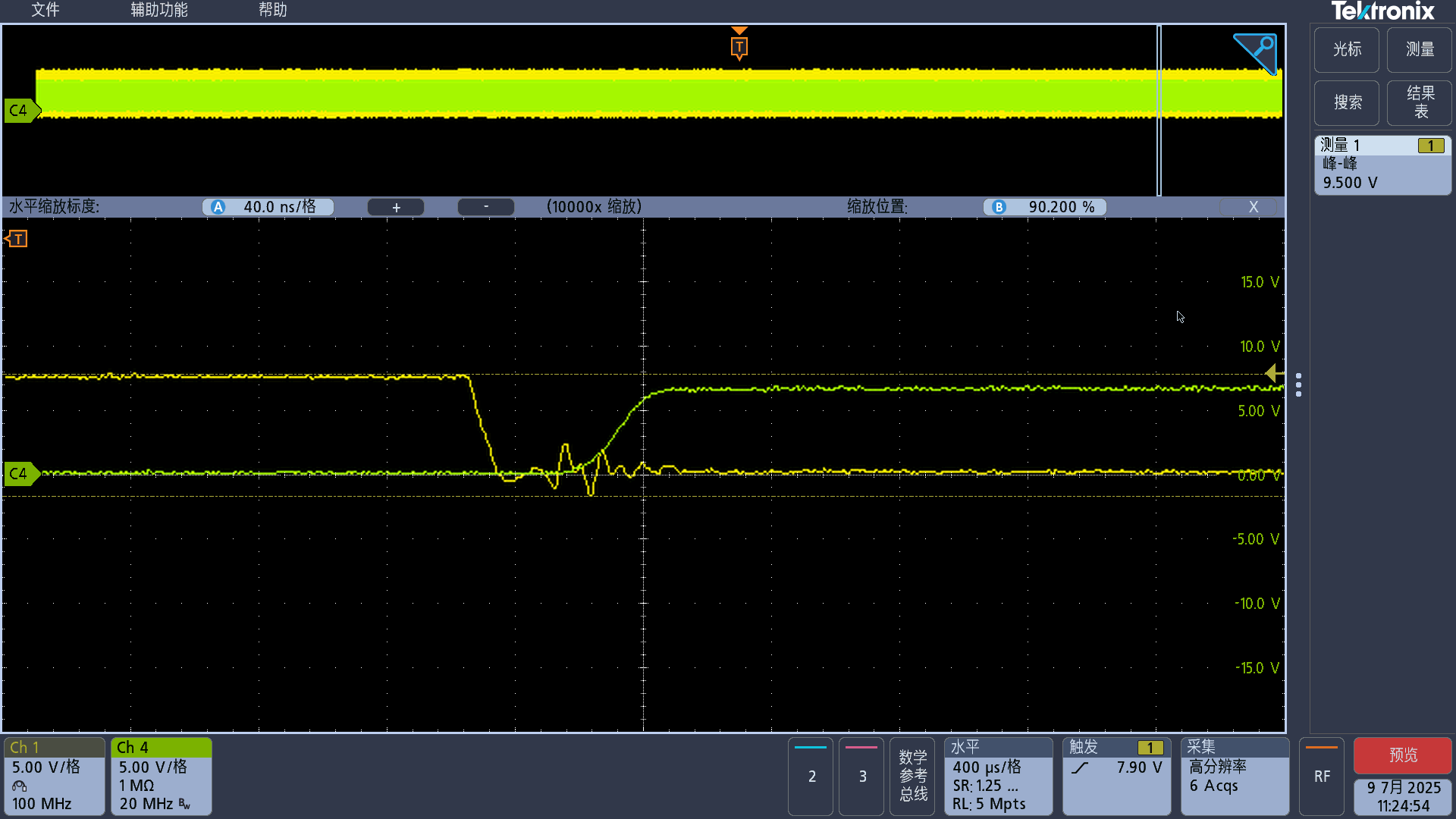
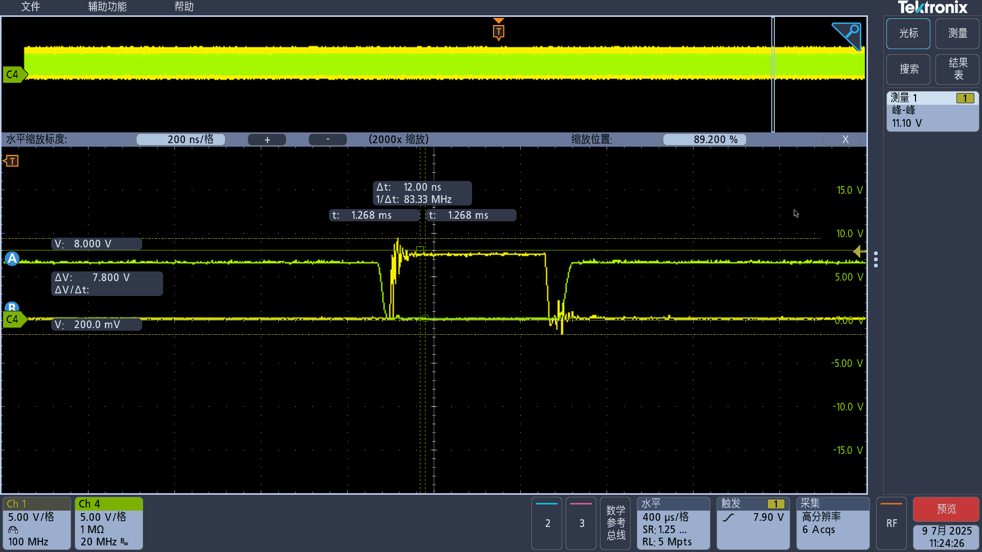
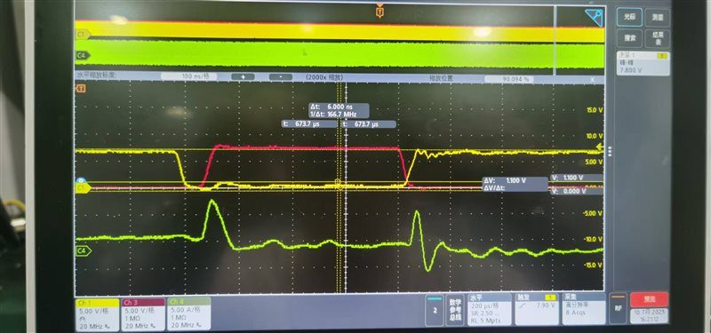
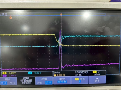
My customer (Enpower) is testing LM5164-Q1 and found THE two MOSFETs of BUCK circuit would be shoot-through by Vgs ringing. Do we have some suggestions to avoid the shoot-through? Thanks.

Best Regards,

Ryker

  • Hi Ryker,

    Please send the schematic and MOSFET part numbers. Are gate resistors installed? There shouldn't be any shoot-through.

    Ringing on the high-side FET gate waveform is due to parasitic gate loop inductance, hence why it's important to route HO and SW together and keep these traces reasonably short (refer to the EVM layout and the layout guidelines in the data sheet for more detail).

    Regards,

    Tim

  • Hi Tim,

    Please refer to below information. Thanks.

    • MOSFET datasheet:

    Yangjie-YJD45G10AQ.pdf

    • LM5146-Q1 PCB Layout:

    PCB Layout of Vgs.zip

    • LM5146-Q1 Schematic:

    • Besides, they also found similar ringing on EVM, and captured waveform as below show:

    Best Regards,

    Ryker

  • Hi Ryker,

    There will be some ringing on LO as SW voltage rises, as current is coupled through Cdg of the FET into the gate and through the internal and external gate resistance. As long as the blip on LO is below the Miller plateau, there is no cross-conduction.

    Try selecting FETs with lower Rgate-internal, preferably in 5 x 6mm package that has much lower parasitic inductance.

    Regards,

    Tim

  • Hi Tim,

    Except of changing the MOSFET, do you have other suggestions to reduce the ringing? Because customer has fixed the MOSFET in current board. Thanks.

    Best Regards,

    Ryker

  • Hi Tim,

    And Enpower also found the cross-conduction issue on EVM as below waveform show. And the test condition is:

    • Vin: 30V
    • Vout: 24V
    • Iload: 0A (there is 1A load in Enpower's own board)

    Best Regards,

    Ryker

  • Hi Ryker,

    How is the current being measured here? If you're showing the HO-SW and LO waveforms here, there isn't any overlpa that would cause shoot-through.

    PS: A buck converter in CCM at no load has a different SW node voltage behavior relative to a loaded condition. The inductor current is largely responsible for slewing the SW voltage, and the deadtime timeouts at ~40ns. What's you're seeing here is likely parasitic capacitive current.

    Regards,

    Tim

  • Hi Tim,

    Except of changing the MOSFET, do you have other suggestions to reduce the ringing? Because customer has fixed the MOSFET in current board.

    Let me clear below waveform: Red is LO, Yellow is HO-SW, Green is current of Q2 (fly-wheel MOSFET)

    R&D also tested the EVM with 1W load and found the similar shoot-through (Peak current is more than 5A too). Does the parasitic capacitive can cause such high current? Could you confirm in EVM and share the test condition?

    Best Regards,

    Ryker

  • Hi Ryker,

    This looks like gate drive current and/or current coincident with the SW voltage transitioning. For example, the current pulse occurs when LO (red trace) goes high, yet HO-SW (yellow trace) is off. Both FETs are definitely not on simultaneously.

    The other transition occurs when LO goes low and HO-SW goes high (minimal overlap here). Please include the SW voltage as well. If there was any shoot-through, it would cause a change in slew rate of the SW voltage.

    How is the current being measured here? Take a look at full load as well....

    These waveforms look pretty clean overall.

    Regards,

    Tim