This thread has been locked.

If you have a related question, please click the "Ask a related question" button in the top right corner. The newly created question will be automatically linked to this question.

LM5116: Negative power source 10V/10A - IC die at 4 A load

Part Number: LM5116

Tool/software:

Hi,

I am designing negative power supply with rating 10 V / 10A from 30 - 40 V, but I am facing strange behavior of LM5116.

We are using it as a symetrical power supply and with positive output we dont have any problem.

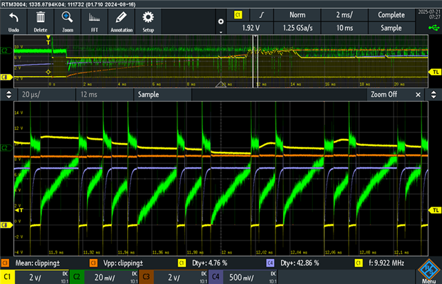
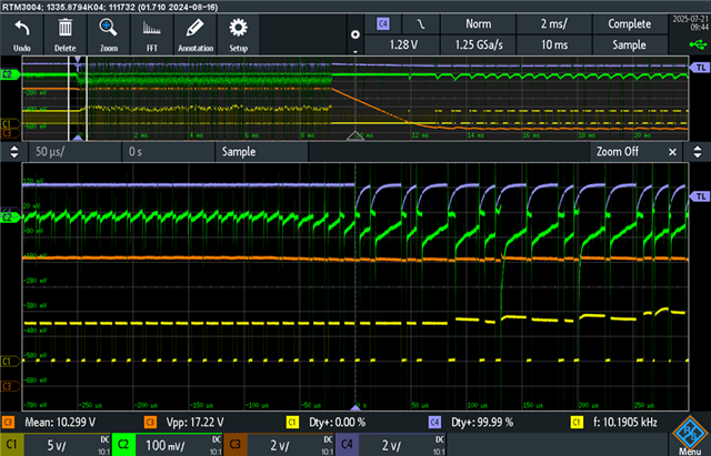
Durring loading Vcc voltage rises to 12V with generating audible noise. After few second driver is defective with LO side driver impedance to PGND less than 10 Ohm.

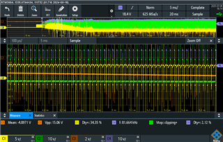
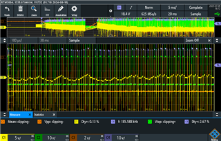
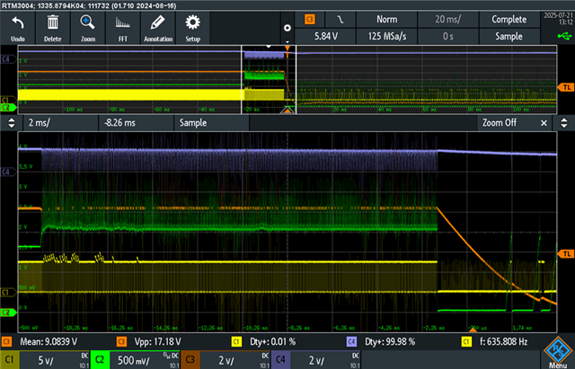
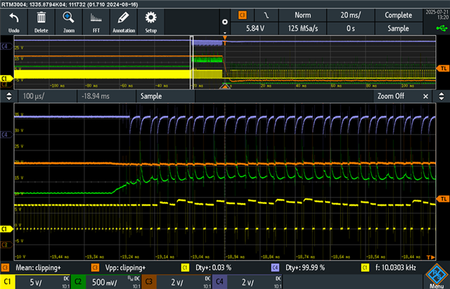
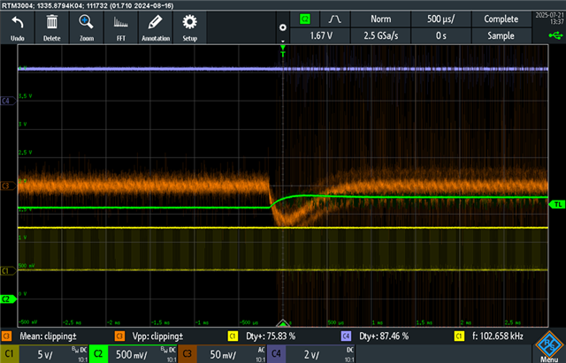
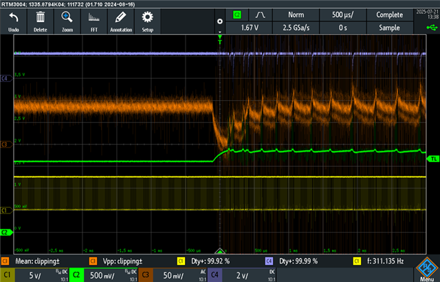
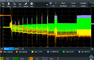
Situation is visible from my measurement 
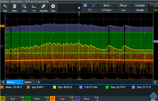
CH1       pin 15 IC2 (LO)

CH2       pin 20 IC2 (SW)

CH3       Negative Vout

CH4       pin 19 IC2 (HO)

detail at 2 A load. There is ringing, but I dont knot how to improve it.

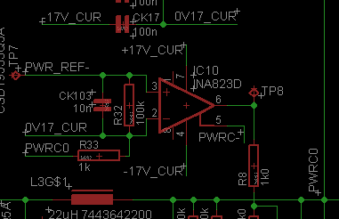
Part of schematic below (output voltage regulation is not implemented at the moment).

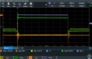
During power on procedure it behave strangely as well. It also generate strange audible noise. It is powered from power transformer with ideal diode bridge (that why there are steps during power on).

Thank you in advance for any suggestion what to test or change.

Feedback is different for positive and negative output and it is based on webench.

  • Hello Michal 

    If you can duplicate the issue easily, please replace D4 diode and check if any improvement. VCC regulation target is 7.4V. It cannot be increased to 12V if there is no external power supply.  

    -EL 

  • Hi,

    I changed D4 to MMBD1503A (200 V/0.2A fast diode) and situation has changed, but problem is still there.

    I also applied UVLO to 20 V (15k and 1k resistor) to prevent switching durring low voltage on input.

    For now driver is not damaged so frequently during testing if I run it just for wes seconds.

    Power on prodecure with CC 2 A load - High voltage on LO and HI pin is visible.

    Power on procedure with 7 A CC load

    Do you have any sugesstion what to test or check?

  • Hello Michal

    I believe the schematic you shared is wrong . VCC regulation target is 7.4V. It cannot be increased to 12V if there is no external power supply at VCC (or at VCCX)  
    Please replace the IC and check if any improvement. If any improvement by replacing the IC, means the original IC was damaged. 

    -EL 

  • Hi,

    Schematic is correct, i can send you complete design including layout in Eagle to PM.

    Situation is same even if we change all semiconductors.

    We see improvement with change of compensation parts on COMP pin.

  • Hello Michael 

    I haven't seen the case the VCC voltage is increased / decreased by changing the COMP components. Anyway, please explain in detail about the COMP component change for my investigation. 

    -EL  

  • I found out that it was probably caused by UVLO divider that was originally 22k and 1k with 1nF capacitor on UVLO pin.

    In this situation with load more than 5 A driver was permanently damaged after few seconds.

    After approx. 4 dips on UVLO pin voltage on Lo pin increased.

     During my measurement i change reference of my scope to negative voltage output (it is possible due to floating design on toroid transformer).

    Original situation on 4 A (electronic load in CC mode - in application note from TI I found out that it is not best solution for power on testing )

    CH1 is Lo side output

    CH2 voltage on shunt

    CH3 is ground of negative output (referenced to negative output)

    CH4 voltage on UVLO pin

    In next step I try to change UVLO divider to 100k and 4k7. After this change driver changed it behavior and wasn't able to power on with electronic load on 4A (only with 0.5 A) but it is probably due to CC mode. Now I trying it in CR mode during power on stage.

    In this situation driver is capable to withstand 10 A load without destruction (it is in overload condition but it recovers).

    Situation with 10A CC load, it is visible that driver output on Lo pin is still increased with dips at UVLO pin. 


    I changed Cramp to 2.2nF and increased frequency to 102 kHz (33k)

    Situation with load step from 0A to 10 A, 

    CH1 is Lo side output

    CH2 COMP output

    CH3 is ground of negative output (referenced to negative output)

    CH4 voltage on UVLO pin

    Now it is probably badly chosen compensation components?

    It looks ok with 4R load

    but 3R load is not ok and it is not stable, sometimes it goes to OCP?

  • Hello Michael 

    What this circuit is for ? You said it is Negative10V power supply, but looks like you are adjusting VOUT.  

    -EL

  • Yes it is for adjusting output voltage, but it is not connected to the circuit at the moment. R31 is not populated.

  • Hello Michal 

    Looks like the converter is overloaded, and then inductor is saturated. Please measure the inductor current using current probe and check if the inductor is saturated. The current limit will be triggered earlier than your expectation if the inductor is saturated. 

    -EL

  • Hi EL,

    It was inductor saturation, after measuring inductor current it was clear. I must change it to only 10uH (same package) with higher saturation current.

    Now I have another issue. In case of 17V on output and 10A output it is desctructive situation when driver, lo side FET and shunt CFG0612-FX-R005ELF (5 mOhm 1W) is destroyed. Normally at 10V/10A it works fine.

    I dont have any osciloscope measurring because I am waiting for new parts to be delivered.

  • Hello Michael 

    Good to hear you found the inductor saturation. 

    The current sense resistor damage is typically caused by an excessive power loss. I guess a wrong sense  resistor is populated now, or there is a situation the load current becomes  >~15A. The power loss is greater than 1W when >15A flows. 

    -EL