This thread has been locked.

If you have a related question, please click the "Ask a related question" button in the top right corner. The newly created question will be automatically linked to this question.

LM25117: LM25117 - Basic Buck Regulator with CC Feature Problems

Part Number: LM25117

Tool/software:

Hi there to all,

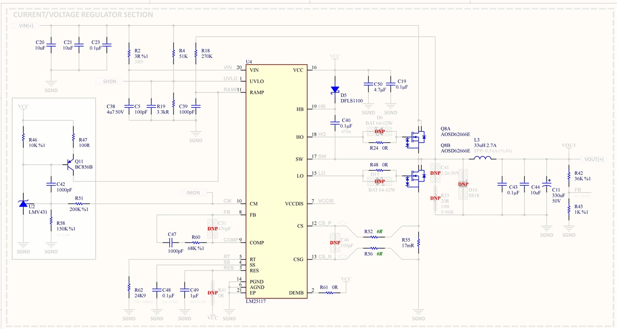
I wanted to obtain a 30V/1.5A CC/CV regulator and designed two variant with LM25117, according to the datasheet page 34 and application note SNVA829 but I have some problems with them. Hence I wish solve them together.

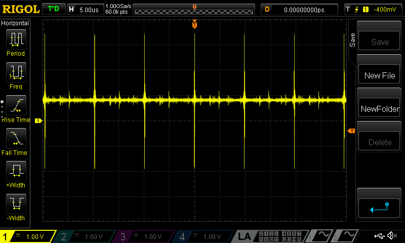
NOTE: There is no overheating generally but the inductor is quite warm at ~ 45C. SHDN and IMON ports are not connected anywhere in the schematics.

For the variant-A that follows the datasheet,

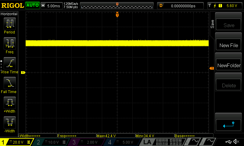
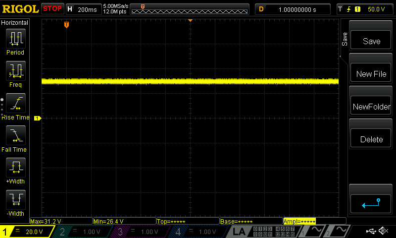
  • For now, output voltage is same as the input that is 36V and output current limit is only limited by the source so there is no CC and CV control. I am still testing and the schematic is shown below.

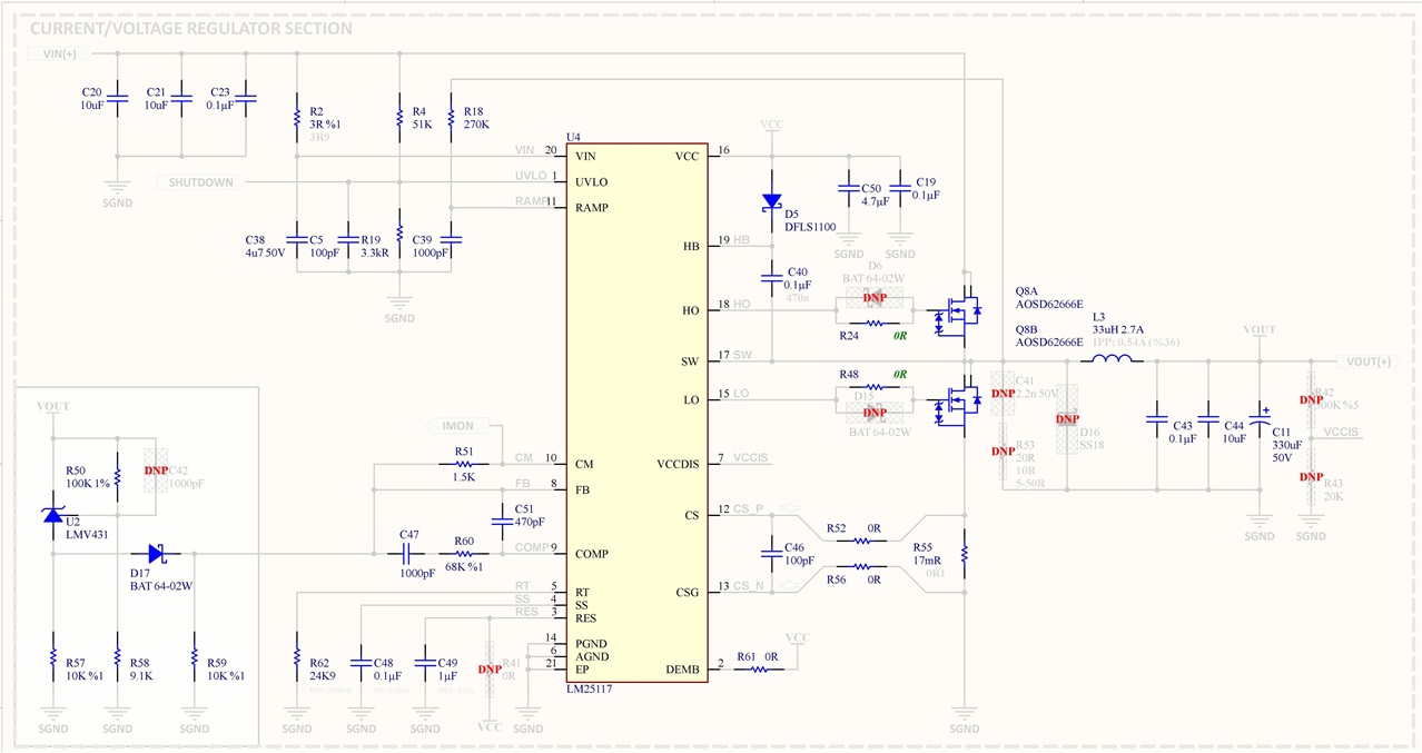
For the variant-B that follows the application note,

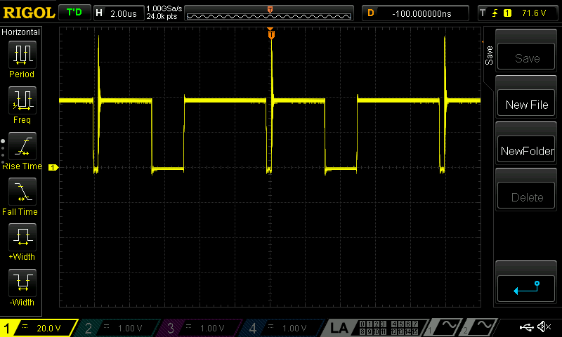
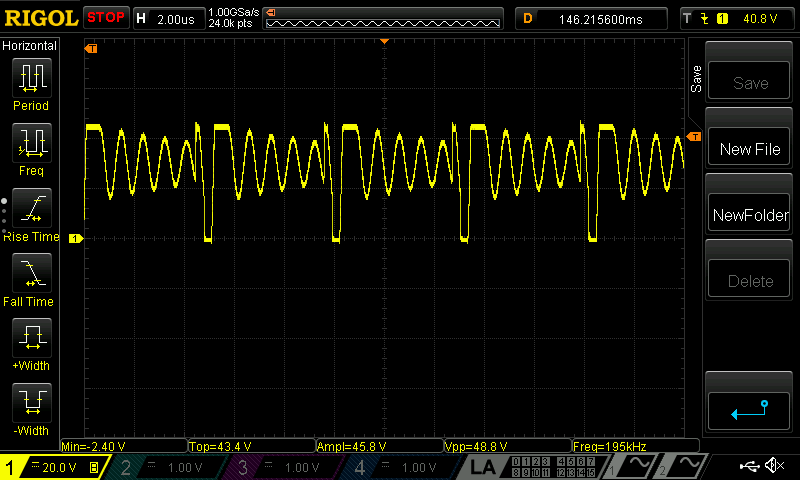
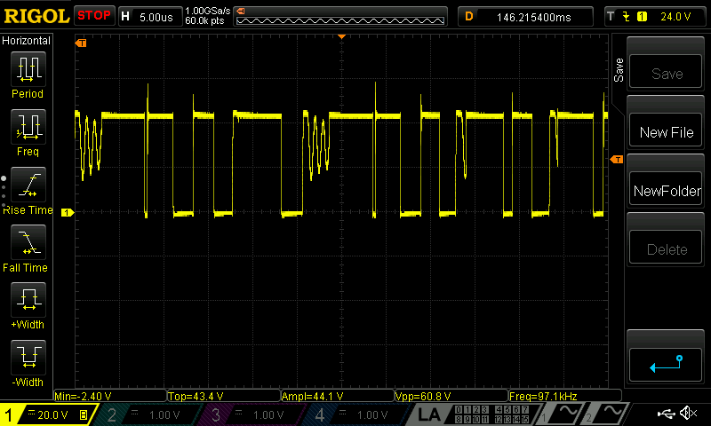
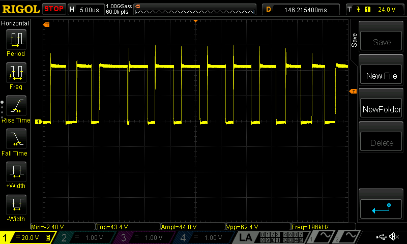
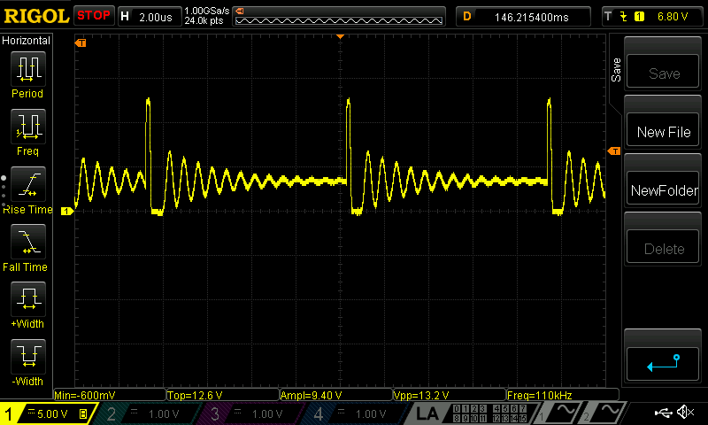
  • For now, I can control the output voltage that is ~30V but when the load current is reaches ~430mA the IC enters the hiccup mode. Somehow it cannot supply more than this level of current and I cannot read any CM output for load current in terms of voltage. For testing, I removed the R51 and Q11 to disable the CC control. The schematic is shown below.

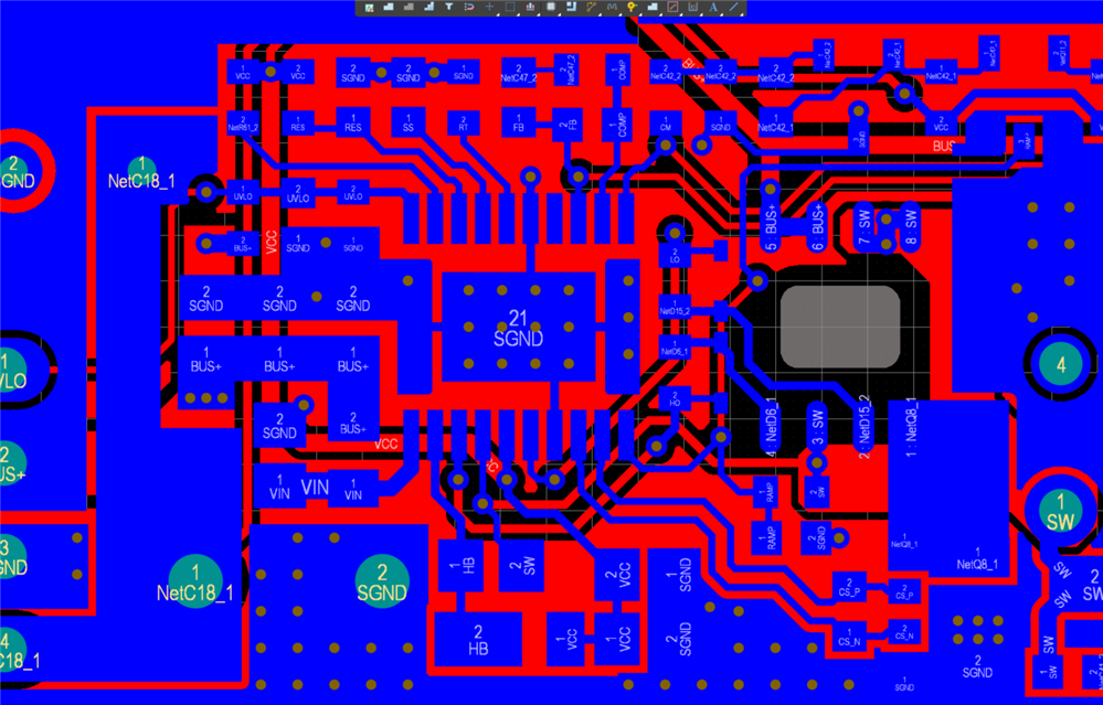
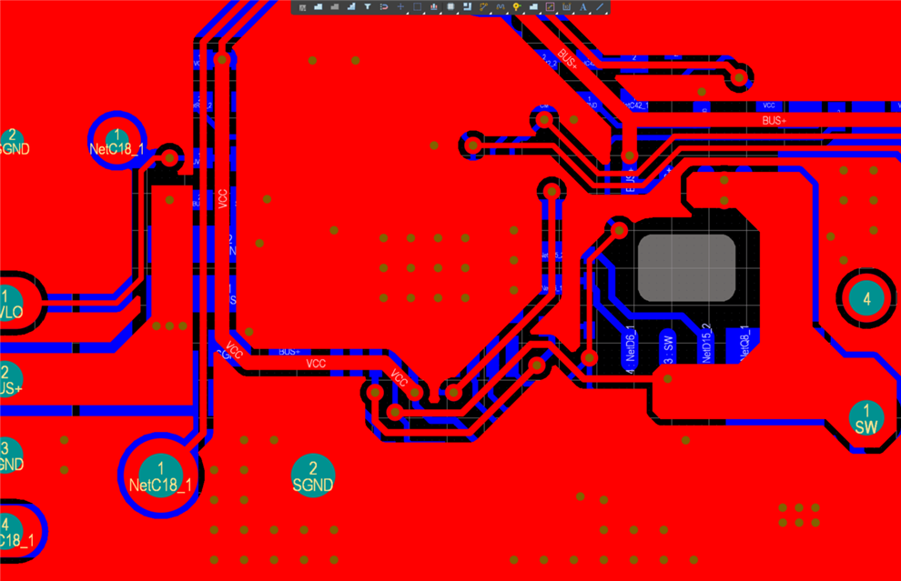
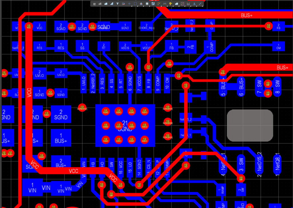
The layouts are quite same and shown below,

I am still testing and waiting for your comments, opinion and experiences.

Thanks for all and have a nice day!

  • Hi,

    Are all your issues related to the CC/CV application, or is there a separate issue with the datasheet application? Please also send screenshots on an oscilloscope of the observed behavior where the device is entering hiccup mode.

    In regards to your layout, can you also include a screenshot of the design with the polygon pours included?

    Thank you,

    Joshua Austria

  • Thanks for your support.

    As I described detailed above, each application has its own issue.

    The layout includes the polygons is shown below.

    I will also send the oscilloscope screenshots.

    Have a nice day.

  • Hi,

    The SGND plane on the top side looks constrained due to the small traces between its pad and the surrounding copper pour. It is important that this pour is not thermally choked.

    Thank you for confirming. I will wait on the oscilloscope shots.

    Thank you,

    Joshua Austria

  • Hi there again.

    Sorry for the delay. After this, we can quickly reply.

    In terms of layout, I saw some bad routing after you. As shown below, SGND from the IC, is traveling only from very thin traces instead of short and suitable track sizes. Can this cause this kind of problem?

    FFrom your perspective, the IC side, should layout be like this?

    For the screenshots, I have VIN, RAMP, FB, VCC, HB, HO, SW and LO signals for IL=300ma and when entered in hiccup mode. Which ones would you like to see?

    By the way, I realized that for VIN=38V and VOUT=29.80V, I can load with 300mA but changed the load to 500mA it enters hiccup mode but not returns from there, even when I disconnect the 500mA load. So I must reset the VIN.

    Also it seems highly depends on VIN. I adjust VIN between 33-38V and it behaves strange by entering the hiccup mode.  

    Thanks for all!

  • Hi,

    Yes, I seem to have missed that. That choke point on SGND is not recommended as it reduces thermal dissipation.

    VIN, SW, FB, and VOUT would probably the best signals to see on a first pass. 

    Do you have an EVM for this device on hand? It may be helpful to do an ABA swap on the EVM to rule out the potential of an IC failure.

    Thank you,

    Joshua Austria

  • Hi there again.

    I have the EVM but ICs seem fine.

    For the layout, I will revise but this may not the responsible for the issue. As you know before, it was entering the hiccup mode after IO~400mA and stay there. But now, I can load it up to 1.5A that I set. I realize this by increasing the input voltage.

    Firstly, while it in hiccup mode I increased the input voltage by 1-2V and it left the hiccup the mode and started to supplying the load current. Then it again entered the hiccup mode when IO~1A and I again increased the input voltage by 1-2V and it left the hiccup the mode and started to continue supplying the load current. Now the VIN increased to 43V and IO: 1.5A without any problem. So seem that there is some kind of inductor issue but according to the calculation tool, 33uH is fine.

    What is your opinion?

    Also the screenshots are shown below. They seem a bit different and noisy but...

    NOTE: All of them taken when IO~300mA.

    • VIN

    • SW

    • FB

    • VOUT

  • Hi,

    Sorry I did not catch this before, but the SW looks to be experiencing considerable ringing. Looking at the SW node on your layout, it is connected to the inductor and FETs through a via and a thin trace. This adds a fair amount of inductance on the high di/dt loop of the controller which will result in more noise. This looks to be affecting your FB pin, which further affects the regulation of the device.

    Can you modify the EVM by populating the components? From there, see if you are seeing similar behavior to your board. If you are not, then we can be more sure that the layout is the culprit as opposed to the component selection. 

    Thank you,

    Joshua Austria

  • Hi,

    I know, the layout is not my best, because of the restricted board area and other chunky TH components.

    Firstly, I am going to try to connect the SW pin with minimum length by using  a wire. Then I am going to try to modify the EVM according to my requirements. But these may take some time. 

    Thank you.

  • Hi Aytac,

    Sounds like a plan!

    Thank you,

    Joshua Austria

  • Hi Aytac,

    As I have not heard from you in some time, I will close this thread for now.

    Should you need further assistance, please feel free to reopen the thread.

    Thank you,

    Joshua Austria

  • Hi again.

    As I have another project, I cannot look at this issue much more. But recently, I got much better results by bypassing the SW signal with a short cable. Below you will see the improved SW signal for different load current.

    • With no load,

    • With 750mA load,

    • With 1500mA load,

    So it seems like related to the layout as you said. But there is one thing that still interesting. Somewhat my SW signals seem mirrored, when compared to the EVM which is shown below.

    • SW signal from the EVM with no load,

    Currently, I cannot investigate in detail as I said before but still I am trying to continue when I found some time.

    I look forward to see your opinion.

    Thanks and have a nice day!

  • Hi, 

    Can I ask how you are measuring SW and where you are grounding the probe? 

    Looking at the no load waveforms, they do seem to be consistent with the EVM direction wise.

    I do agree, this is likely an issue with the SW node layout. I will also note that as you are using a wire, this does still add extra impedance and inductance. Our best recommendation would be to do a layout revision to solve the SW node spikes and pull them more inline with the EVM waveforms.

    Thank you,

    Joshua Austria

  • Hi.

    I'am taking the GND node as close as possible to the SW node.

    I know the possibbe problems related to the wire, so it was just testing. At the end, it seems that the layout will be revised.

    But for no load waveforms, I am seeing that my waveform is vertically flipped when compared to the EVM. (Except the longer ringing.)

    Thanks for your support.

  • Hi Aytac,

    Oh I see what you are referring to. Are both devices operating in PFM mode? It also looks like they may be operating at different operating conditions. What are the operating conditions (VIN, VOUT, FSW, and mode) that the device is being used in on your layout versus the EVM?

    Thank you,

    Joshua Austria

  • Hi Joshua,

    Sorry for the delay.

    The design is according to the completely parallel to to the EVM, with some different component values for different VIN and VOUT.

    You can see the schematics from the previous posts. But I removed the CC/CV sections for testing with EVM.

    VIN: 36.0V, FSW: 216kHz, VOUT: 29.7V, MODE: I did not set any other mode, just as in the EVM.

    What are your first your opinions about the mirrored SW signals? I do not expect that comes from the layout but I wonder what can cause this? 

    Thank you and have a nice day.

  • Hi Aytac,

    It does look like the EVM and your board are operating at different conditions. SW in the EVM photo only reaches 12.6V max whereas the SW in your board is reaching 45.8V, which is above the ABS MAX for this part. I believe it would be best to equalize the test conditions for both boards to get an accurate comparison of the no load SW signal for both of these devices.

    What you are seeing with the EVM is that in a low load condition, the device is operating in PFM mode, reducing its switching pulses to help with efficiency. The device will pulse the high side, experience a deadtime where both FET's are off, and then recover. It does look like the same thing is happening with your board, but the high side FET on-time is less apparent as you have a higher input voltage. It may look mirrored, but I believe if you were equalize your application to the EVM, you would see the operation match closer to the EVM conditions.

    Thank you,

    Joshua Austria

  • Hi again,

    For SW pin, I was check during the design and there were no problem. You can see the below which belows the other SNVA466B EVM board whose only VIN and VOUT are much more than the SNVA469B and see the SW signal which is going to 50V) Am I interpreting wrongly?

    In terms of working conditions, they must be same, because of the schematics. Differences are only for different VIN and VOUT. So unless there are some calculation issues for compensation network and sense resistor, it should be work. For now, I do not have the inductor but I will try to do as you said to compare both.

    Thanks for all.

    Have a nice day.

  • Hi Aytac,

    Yes, SW should essentially reach VIN when you are operating. However, your scope is saying that you are reaching 42.6V when you have a 36V input. I believe that your layout and subsequent measurement technique to be adding considerable impedance to your SW node, which is causing you to see those intense spikes that are not on the EVM. 

    Past this however, the reason I am mentioning the differences in the application parameters between the EVM and your board is that the differences in VIN and VOUT can cause the differences in the SW node waveforms as you see there. Without equalizing the application parameters, it is difficult to ascertain what differences in SW node is a result of your different application parameters or your different layouts.

    Thank you,
    Joshua Austria