Tool/software:
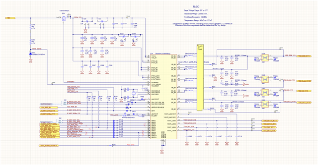
Using TPS6594133ARWERQ1, for jacinto board
PMIC has input voltage and enable event/level
However no output voltages are seen,
EN_DRV is low lighting the fail safe LED
GPIO9 can be forced low or high, with no change.
No oscillation seen on OSC32
| 1 | Floating | AMUXOUT | |
| 2 | 1.80V | LDO_INT | |
| 3 | 1.80V | LDO_RTC | |
| 4 | 3.30V | VCCA | |
| 5 | 0V | GND | |
| 6 | 0V | GND | |
| 7 | 0V | LDO4 | |
| 8 | 3.30V | PVIN_LDO4 | |
| 9 | 0V | LDO3 | |
| 10 | 3.29V | PVIN_LDO3 | |
| 11 | 735mV | LDO2 | |
| 12 | 3.30V | PVIN_LDO12 | |
| 13 | 0V | LDO1 | |
| 14 | 0V | nINT | |
| 15 | 0V | SW_B2 | |
| 16 | 0V | SW_B2 | |
| 17 | 3.30V | PVIN_B2 | |
| 18 | 0V | GPIO7 | |
| 19 | 3.30V | GPIO9 | |
| 20 | 0V | nPWRON | |
| 21 | 0V | FB_B2 | |
| 22 | 0V | FB_B1 | |
| 23 | 0V | GPIO5 | |
| 24 | 0V | GPIO6 | |
| 25 | 0V | nRSTOUT | |
| 26 | 3.30V | PVIN_B1 | |
| 27 | 0V | SW_B1 | |
| 28 | 0V | SW_B1 | |
| 29 | 0V | EN_DRV | |
| 30 | 3.30V | SDA | |
| 31 | 3.30V | SCL | |
| 32 | 734mV | GPIO1 | |
| 33 | 734mV | GPIO2 | |
| 34 | 0V | SW_B5 | |
| 35 | 3.30V | PVIN_B5 | |
| 36 | 0V | VBACKUP | |
| 37 | 0V | FB_B5 | |
| 38 | 0V | O32_I | |
| 39 | 0V | O32_O | |
| 40 | 1.80V | O32CAP | |
| 41 | 0V | GPIO8 | |
| 42 | 40mV | GPIO10 | |
| 43 | 0V | SW_B3 | |
| 44 | 0V | SW_B3 | |
| 45 | 3.30V | PVIN_B3 | |
| 46 | 0V | GPIO3 | |
| 47 | 0V | GPIO4 | |
| 48 | 3.30V | VIO_IN | |
| 49 | 8mV | FB_B3 | |
| 50 | 59mV | FB_B4 | |
| 51 | 3.30V | VSYS_SENSE | |
| 52 | 8.89V | OVPGDRV | |
| 53 | 0V | GPIO11 | |
| 54 | 3.30V | PVIN_B4 | |
| 55 | 50mV | SW_B4 | |
| 56 | 50mV | SW_B4 |
My questions are,
1/ does this p/n come with a factory pre-programmed configuration ?
2/ Does this pre-programmed configuration have some documentation as to the expected behavior ?
3/ Are the LDO's expected to be off ?
4/ Is the OSC32 expected to be off in this config ?
5/ Forcing a 0 or 1, into GPIO9 assuming it is a watchdog disable function,
Applying a 0, or 1 onto nPWRON/ENABLE (which is it for the pre-programmed config ?)
does not alter no power output
6/ Any ideas on debug
I ordered a launchpad 432 and EVM for this part so I can play with one out of circuit, and attach in circuit
but any insight appreciated.
On the other hand, If I assume this part is not factory pre-programmed, things make a bit more sense. However, then,
Can I get the setup as used in the EVK p/n as mentioned in the schematic clip
Schematic is similar to the eval kit for jacinto