


Other Parts Discussed in Thread: TPSM82810, TPSM82813
Tool/software:
Hi.
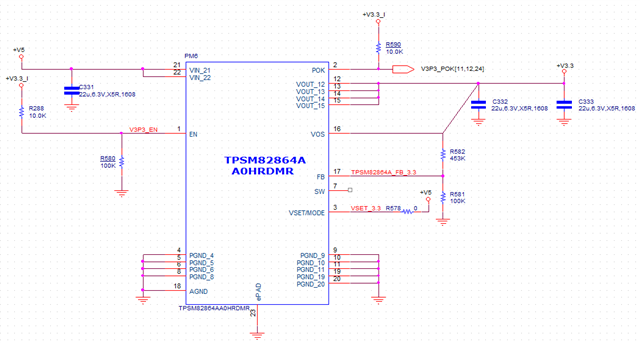
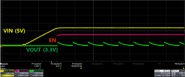
I designed a 5V to 3.3V circuit using TPSM82864AA0HRDMR.
I have a problem with the 3.3V output waveform.
What should I check?
Best Regards
Tool/software:
Hi.
I designed a 5V to 3.3V circuit using TPSM82864AA0HRDMR.
I have a problem with the 3.3V output waveform.
What should I check?
Best Regards
