This thread has been locked.

If you have a related question, please click the "Ask a related question" button in the top right corner. The newly created question will be automatically linked to this question.

UCC28180: UCC28180

Part Number: UCC28180
Other Parts Discussed in Thread: TIDA-00443

Tool/software:

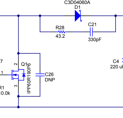
Subject: Clarification on CE Emission Compliance & Support for UCC28180-based 650W PFC Design

Dear TI Support Team-,

Dear Tom,

We are currently using the UCC28180 PFC controller in one of our designs with the following specifications:

  • PFC Output Power: 650W

  • Input Voltage Range: 165Vac to 280Vac 
  • Output Voltage: 396VDC

  • Switching Frequency: 70kHz

We are facing an issue during Conducted Emission (CE) testing as per EN 55014-1 Class B. The CE test results show peaks in both Quasi Peak and Average levels in the frequency range of 9 MHz to 16 MHz.

To analyze this, we referred to TI’s reference design TIDA-00443 (900W PFC design). In the CE results for TIDA-00443, we observe emissions peaking around 18 MHz to 30 MHz. However, the reference guide does not clearly mention whether the results pertain to Class A or Class B compliance. Could you please clarify this?

Additionally, please find attached our CE test results (PDF) for reference.

We would also like to know:

  1. Does TI offer any reference design compliant with EN 55014-1 or EN 55032 Class B for power levels ≥500W, ideally around 650W?

  2. Are there any updates or design guidelines for UCC28180 specifically addressing CE compliance?

  3. Any recommendations for filtering or layout changes to reduce the 9–16 MHz conducted emissions?

We appreciate your support and look forward to your guidance.

Best regards,
BR Kadam

  • Dear Team and Tom,

    please revert back on the listed queries on UCC28180. please refer the CE scan. 

    4212.CE Observation PFC 650W ( UCC28180) RV01.pdf

  • In general, the noise in this freq range is coming from high dv/dt and di/dt on the switching node. 

    Please try to minimize the current/voltage loop in layout and consider adding or modifying the snubber components shown below. The FET selection also plays important role here.

    Best,

    Ning

  • Dear Ning, Thank you very much for your feedback.

    Taken trails with RC snubber across Boost diode ,

    1. R = 44E, C= 330P

    2. R = 44E, C = 100P  ( As Cj of Diode is 20 pF)

    There is no heating of snubber Resistor observed during testing.CE Observation PFC 650W ( UCC28180) RV02-21072025.pdf

    CE Results are fail in the Frequency range of 3 to 5 MHz and at 14 MHz. Please refer the  CE Scan 

  • If the snubber is not effective, we need to dig deeper. 

    EMI is a system level issue. Layout and filter component selection play big role here.

    Can you share their layout and BOM selection?

  • Dear Ning Tan,

    Good Evening,

    PFC Converter Specifications – 650W

    • Input Voltage: 230 VAC
    • Output Voltage: 396 VDC
    • PFC Switching Frequency: 70 kHz

    Input Filter Configuration

    A two-stage EMI input filter was implemented with the following component specifications:

    • Y2 Capacitors:
      • C3, C8 = 2.2 nF
      • C5, C8A = 220 pF
    • X2 Capacitors:
      • C1, C2 = 820 nF
      • C5 = 220 nF
    • Common-Mode Chokes:
    • L1, L2 = 2.2 mH / 4 A
    • Part Number: 744823422

    please refer the Input Schematic DetailsInput Filter Component Selection PFC 650W RV01 -21-07-202.pdf

  • Hello BR Kadam, 

    Firstly, the TIDA-00443 reference design CE results are compliant with Class A levels of EN 55011 (Group 1) as noted in the text paragraphs above Figures 33 and 34 in the Design Guide and the limit lines within the CE figures.  The figure captions for Figures 33 and 34 incorrectly attribute compliance to Class B limits.  The CE results for TIDA-00443 do not meet Class B limits.  The captions contradict the text and the captions are wrong. 

    The RC snubber trials which you performed on your design used values based on the TIDA-00443 design and its schematic.
    In your test results there is small but noticeable increase in ~14MHz QP noise in Trial 2 (with 100pF) compared to Trial 1 (with 330pF). 
    This indicates that the snubber across the boost diode does have some influence on the high frequency noise, but not enough for your system. 

    The snubbing for your system should be tailored to the components used in your system, not simply a copy of the TIDA design unless you are actually using a all the same components of the TIDA design.  
    I suggest to also consider adding a snubber across the switching MOSFET and modify the dV/dt and/or dI/dt associated with the MOSFET switching. 

    For snubber resistor temperature rise, I expect the power loss to be = 1/2 * Csnub * 400V^2 * 70kHz = ~1.85W with 330pF cap.
    A 2W-rated resistor should definitely become noticeably hot with that much dissipation. 
    Please check your snubber connections to make sure that the R-C is actually attached across the diode. 
    Also check the resistor value to verify that it is(was) 44ohms and not some value much higher by mistake.

    Regards,
    Ulrich

  • Dear Ulrich,

    Thank you for your detailed observations and suggestions regarding the RC snubber trials and clarification on Class A and Class B CE Test result in TIDA-00443 reference design.

    Snubber component values used in the initial trials were derived from the TIDA-00443 reference design, as shared by E2E forum Team,

    • The physical placement of the R-C snubber is across the diode.

    • The actual resistor value in the circuit to confirm it is 44.6Ω (measured Value).

      I am seeking your support on the next steps regarding EMI optimization.

      Based on your valuable input, I would like to proceed with further tuning of the snubber values tailored specifically for this design, rather than relying on the TIDA-00443 reference values. Your guidance on this approach, as well as on the associated input filter component values, would be highly appreciated.

      Additionally, I would appreciate your feedback on the current input filter configuration with respect to meeting CE requirements, specifically for Class B conducted emissions criteria.

      Looking forward to your suggestions and recommendations.

      Regards, BR Kadam

  • Hello BR Kadam, 

    In-depth support for Emissions Compliance is beyond the purview of this E2E forum, which is intended to support the proper use of TI power controller ICs.

    Here is a link to a TI white paper concerning conducted EMI in general, but has several links to related topics at the end of the paper: https://www.ti.com/lit/pdf/sszt673?keyMatch=CE%20compliance&tisearch=universal_search&f-technicalDocuments=Technical%20article 

    I suggest to further search TI's website for conducted EMI-related articles and technical documentation. 
    I also suggest to search the web for such information which will be very useful to you. 

    All that said, I suspect that the 14MHz noise is likely to correlate to the dv/dt of the MOSFET drain. 
    This dv/dt, coupling through the winding capacitance of the boost inductor, may be injecting HF noise currents onto the input line, which your EMI filter is not effectively blocking.  This is only my suspicion, not an actual diagnosis, but I suggest to follow up on these points to see if you can mitigate the noise. 

    Regards,
    Ulrich

  • Subject: Request for Further Input on EMI Filter Design and Snubber Network Impact

    Dear Ulrich,

    Thank you for your prompt response and for sharing the white paper on conducted EMI, along with your helpful suggestions. I appreciate the clarification regarding the E2E forum’s scope and understand its limitations.

    Your insights regarding the possible correlation between the 14 MHz noise and the MOSFET drain dv/dt are valuable. I will further investigate the coupling path through the inductor's winding capacitance and evaluate the effectiveness of the current EMI filter configuration.

    That said, I would appreciate your feedback on the existing input filter design, specifically regarding its ability to meet CE Class B conducted emissions requirements. If possible, please suggest appropriate input filter components or topologies that could help in this regard.

    Additionally, I have conducted trials using RC snubber networks across the boost diode (based on a junction capacitance of 20 pF) and MOSFET (based on Coss = 1500 pF, Qrr = 9 uC). Various combinations were tested with R = 44 Ω, 47 Ω and C = 100 pF, 330 pF, and 470 pF. However, the introduction of these snubbers appears to have increased the number of peak emissions observed in the lower frequency range (150 kHz–290 kHz), as well as in the 3–5 MHz, 14–15 MHz, and 27–28 MHz bands.

    Could you please share your thoughts on this behavior and suggest whether any tuning or redesign might be advisable?

    I will also continue exploring relevant resources on TI’s website and beyond, as you recommended. If possible, could you share specific links or documents that address CE compliance or Class B conducted EMI mitigation more directly?

    Looking forward to your suggestions and further recommendations.

    Thank you once again for your support.

    Best regards,
    BR Kadam

  • Hello BR Kadam, 

    I have to reiterate that your questions are beyond the purview of this forum. 

    I recommend to conduct a Google search on "RC snubber design" and check out the many responses that address this topic.  Some from TI and many from other companies.   The same can be said for searching for EMI filter design.

    Keep in mind that the purpose of an RC snubber is to dampen ringing of a series L-C network or a parallel L-C network. 
    In a PFC topology, the ringing is typically due to a series L-C network, but not always.  The optimal damping resistance value depends on whether it is series or parallel.  

    The choice of snubber capacitance is usually 3X the value of the total capacitance on the ringing node. The total capacitance is the sum of the MOSFET, diode, inductor, and stray capacitances.  Also, semiconductor junction capacitances can be highly non-linear, and should not be assumed to be a single value form the device data sheet.   Find the capacitance curve for each part and get the value at the voltage where the ringing happens.   

    Don't assume that your EMI filter components are ideal.  Each part has parasitic elements that degrade performance at certain frequencies. 
    Inductors (CM and DM) have winding capacitance that allow high frequency currents to by-pass the inductive impedance. 
    Capacitors (X and Y caps) have lead inductances that inhibit the conduction of high frequency currents through them.
    Undamped L-C ringing within the EMI filter may exaggerate certain noise frequencies. 

    All of these aspects should be considered and investigated to optimize a filter's effectiveness over the full conducted-EMI range. 

    Regards,
    Ulrich