


Tool/software:
Dear TI Experts,
Here is question about boost topology of LP8866S-Q1:
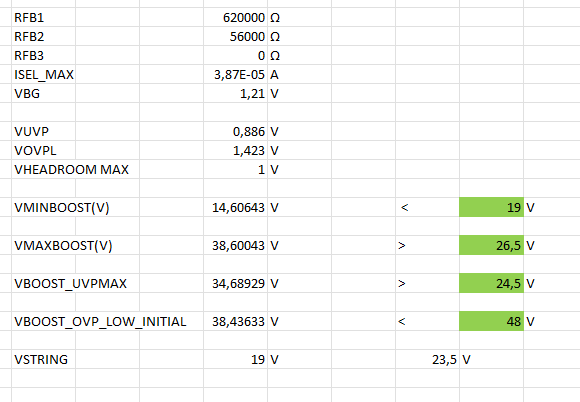
As I checked datasheet and application note which shown that the feedback resistive divider (RFB1, RFB2, RFB3) defines both the minimum and maximum adaptive boost voltage levels, as well as UVP and OVP levels. Now you can see my design parameters as follow:
If I set input voltage to 28V, I guess the boost controller is not work ,because the input voltage (28V) is higher than Vstring (19v to 23.5V) , in this situation , I would like to know whether the output voltage is approximate to 27V(consider some drop voltage on inductor and diode)and the max. 8V (27V-19V=8V)drop voltage will add on OUTx of LED driver.
I am not sure if my understanding is correct, if not , please correct me .
And my question is if I set input voltage to 27V , the LEDs can work normal or not? if it will trigger OVP ? If the input voltage will impact to UVP and OVP threshold value when the boost controller is not work?
Thanks a lot!
