Other Parts Discussed in Thread: LM7480
Tool/software:
Hi TI team.
Previously, I asked Common drain ORing design concept : LM7480-Q1: Common drain ORing concept
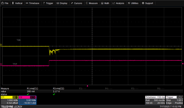
When I measure VMAIN_OUT voltage on the disabled LM7480 ICs, the value is abnormal.
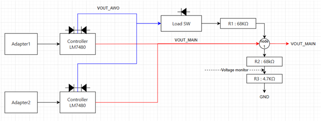
For more detail information, see the diagram.
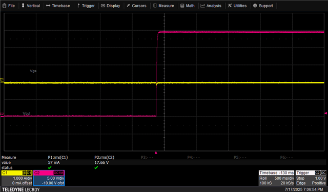
<Test step>
1. No application load.
1. Adapter 1 : attached. 48V.
2. Adapter 2 : detached.
3. Both of LM7480 : Not enabled
4. VOUT_AWO : 48V (from 1st FET body diode)
5. Enabled Extra Load SW at VOUT_AWO line.
6. R1 resistor upper side measured : 48V
7. node1 measured : 2.67V. ??? I expected 24.8V by voltage divider.(68k//(68k+4.7k)
Suspected point.
1. VOUT_MAIN node is connected to the OUT pin of LM7480 IC.
2. VOUT_MAIN is not connected to any other node.
3. The body diode of 2nd FET(LM7480) isn't conducting current because common drain is higher (=48V).
So I think VMAIN_OUT current is flowing into the OUT pin of the LM7480 IC. what am I missing for debugging?
Thank you.