This thread has been locked.

If you have a related question, please click the "Ask a related question" button in the top right corner. The newly created question will be automatically linked to this question.

UCC27211: Glitches on HO, highside MOSFET is turning off too early

Part Number: UCC27211
Other Parts Discussed in Thread: UCC27212

Tool/software:

Hello, 


I am experiencing Glitches with my DCDC Converter which cause the Highside MOSFET to turn off earlier than the HI Signal. 

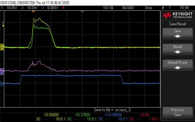
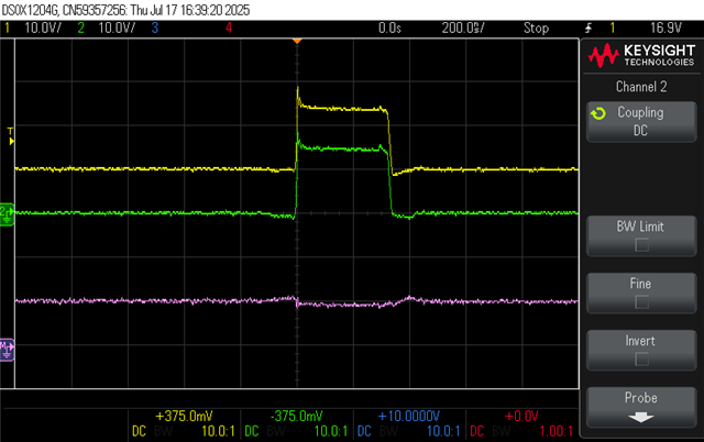
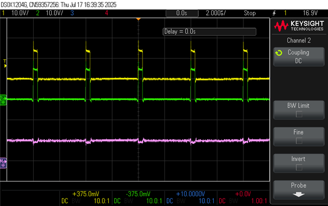
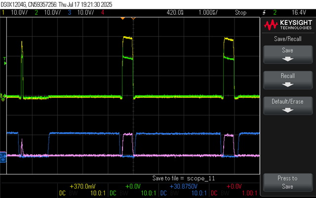
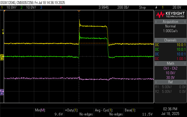
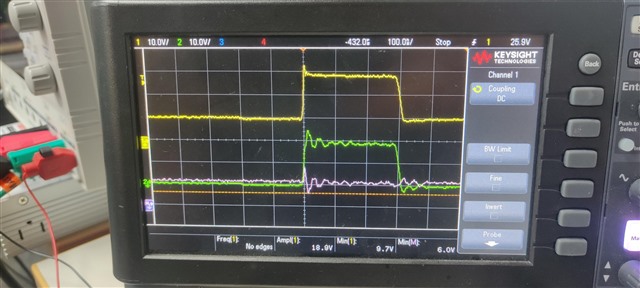
Normal Pulse (200ns)

  • CH1 = HS - GND
  • CH2 = HO - GND
  • Purple = HO-HS


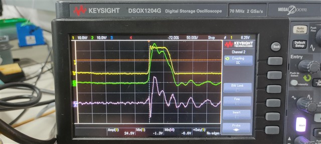
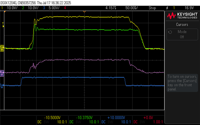
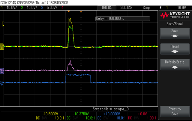
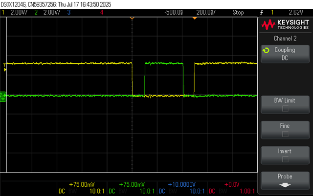
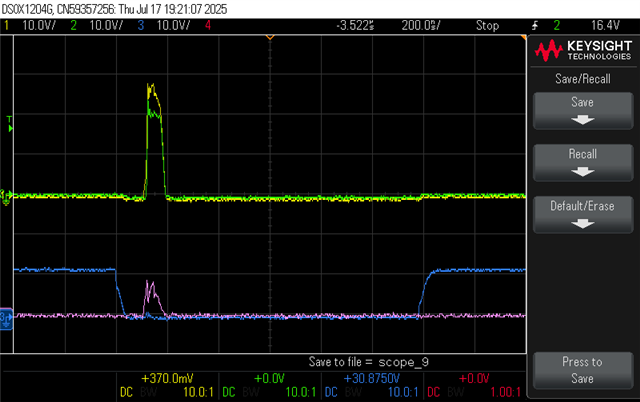
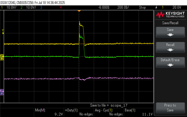
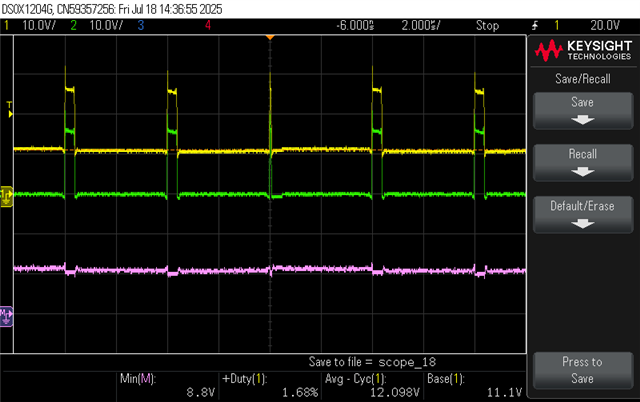
Abnormal Behavior (70ns)

  • CH1 = HS - GND
  • CH2 = HO - GND
  • Purple = HO-HS


Right now i am suspecting 2 different possibilities:

- The UVLO of the Gate driver is turning off HO

- The HO Gate oscillations are going low enough to turn off the MOSFET and it is not turning on again afterwards (because the Bootstrap capacitor is discharged?)


What i have tested yet:

- HI and LI seem to be stable, i measured HI and LI against GND near the Gate Driver. While the length of the Pulse on HI and LI stay stable, the Pulses on HO are sporadically shorter.

- Bootstrap capacitor: I am using a 100nF Capacitor which i have soldered directly to the Pins HB and HS. Before, I had a 100nF and 1uF Capacitor in parallel on the underside of the PCB, connected with vias to the HB and HS Pins

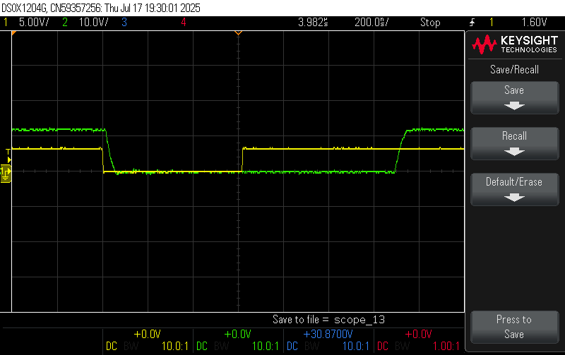
I measured the voltage on the Bootstrap capacitor. It does seem to drop lower than the UVLO threshold, but I am not sure if the UVLO is activating in this short timeframe. Somewhere else I read about a 1us delay on the UVLO.
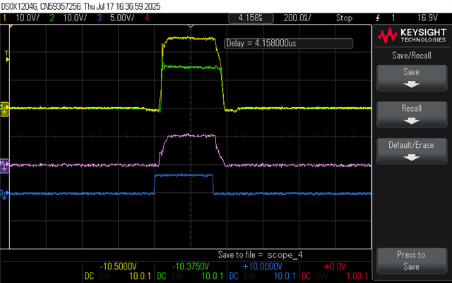
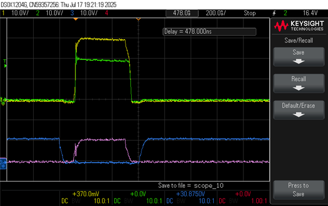
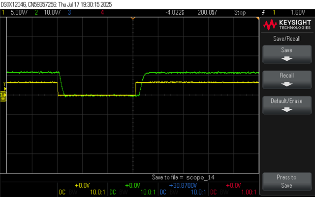
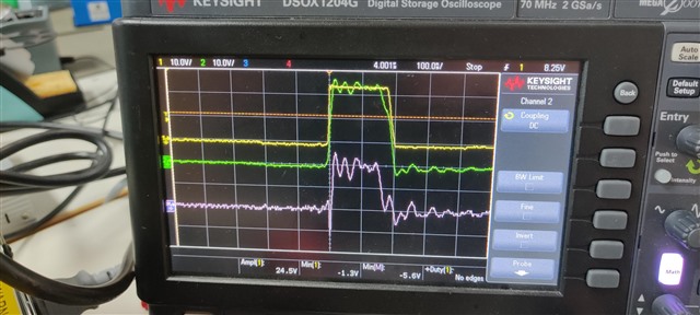
Bootstrap capacitor

  • CH1 = HS - GND
  • CH2 = HB - GND
  • Purple = HB-HS


- VCC: I measured the voltage on the VCC capacitor. I am using a 1uF Capacitor. The Voltage on the VCC Pin seems to stay stable


- Gate Resistance: I experimented with different Gate resistors. A gate resistor higher than 5 Ohm seems to improve the behavior. From this I conclude that abnormal behavior is somehow caused by oscillations on the HS gate. The traces of HO and LO are quite long which are causing a high inductance. 

 board-power_stage_2.pdf


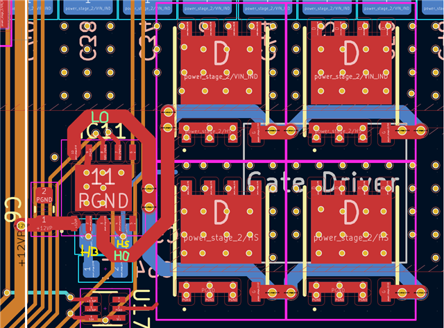
In the next iteration of my design i am planning to shorten HO and LO traces as much as possible. Furthermore, the Bootstrap capacitor will be placed on the upper side next to the Gate driver and decreased to 100nF. 
But I am still trying to figure out the root cause of this problem. Can this behavior be caused by the UVLO? Or are the oscillations of the Gates the cause of the Mosfet turning off. 


Your help is much appreciated

Best regards
Lars Pfueller

  • Hey Lars,

    Thank you for reaching out to TI with your questions regarding the UCC27211.

    Looking at the first two waveforms shared, the HS waveforms appear to be okay but there is definitely some noise seen in the HO and HO-HS waveforms. What probe are you using to measure HO-HS? All of these measurements need to be taken at the pins of the gate driver with high bandwidth probes and utilizing the tip and barrel method of measurement when possible.

    1. Please take these waveforms again considering the recommendations above and also including the HI waveform.

    2. The minimum pulse width spec for this part is 40ns, so any input pulses shorter than that can expect to see shorter or no outputs.

    3. Please reference the schematic review template that is linked on the product page when doing your next board iteration. In short, I would advise RC filters on the inputs, having gate resistors populated for HO and LO, having the HO, LO and HS traces be short and sufficiently wide, placing the VDD and bootstrap capacitors as close to the drivers as possible and sizing them based on this application note: Bootstrap Circuitry Selection for Half-Bridge Configurations. If you would like us to do a full schematic and layout review for that iteration, you can make an e2e thread for that and we can advise.

    4. Looking at the 200ns waveform, HO falls some before the HS falling edge and therefore HO-HS goes low also. For the 70ns waveforms, the oscillations on HO go low and so HO-HS does as well. When taking these, it may be helpful to put HO and HS on the same scale and line them up vertically to see how HO vs HS in comparison to the HO-HS waveform.

    Let me know if there are any questions.

    Thank you,

    William Moore

  • Hello William, 

    thank you for the quick response. 

    I am using the Keysight N2140A passive Probes set to 10x

    - I was able to capture better waveforms which include HI and lined them up according to your description

    Normal Pulse 

    • CH1 (Yellow) = HO - GND
    • CH2 (Green) = HS - GND
    • CH3 (Blue)    = HI - GND
    • Math (Purple) = HO - HS

    Abnormal Behaviour

    • CH1 (Yellow) = HO - GND
    • CH2 (Green) = HS - GND
    • CH3 (Blue)    = HI - GND
    • Math (Purple) = HO - HS

    -----------------------------

    Bootstrap Caspacitor (100nF)

    • CH1 (Yellow) = HB - GND
    • CH2 (Green) = HS - GND
    • Math (Purple) = HB - HS

    -------------------------------

    PWM Input (Deadtime 100ns)

    • CH1 (Yellow) = LI - GND
    • CH2 (Green) = HI - GND

    ------------------------------

    Normal Pulse 

    • CH1 (Yellow) = HO - GND
    • CH2 (Green) = HS - GND
    • CH3 (Blue)    = LO - GND
    • Math (Purple) = HO - HS

    Abnormal Behaviour

    • CH1 (Yellow) = HO - GND
    • CH2 (Green) = HS - GND
    • CH3 (Blue)    = LO - GND
    • Math (Purple) = HO - HS

    ------------------------------------------

    Normal Pulse 

    • CH1 (Yellow) = LI - GND
    • CH2 (Green) = LO - GND

    Abnormal Behaviour

    • CH1 (Yellow) = LI - GND
    • CH2 (Green) = LO - GND

    -------------------------------------------

    - It seems like the Gate driver is somehow turning off. LO is staying low longer than the LI Pulse

    - The Supply Voltage at the VDD Pin of the Gate Driver is stable at 12V

    Best regards and thank you for your support

    Lars Pfueller

  • Hey Lars,

    Thank you for the updated waveforms.

    This is an unexpected behavior and appears to be like a UVLO condition but with VDD pin being stable at 12V, that would not cause UVLO. Is HB-HS still dipping to 6V (below UVLO) during this condition? There is definitely some ringing on the outputs and this is likely due to overshoot and the lack of gate resistors.

    Are you seeing any damage conditions during this?

    Thank you,

    William Moore

  • Hello William,

    I checked HB-HS again while the glitch is happening. It doesn’t seem to drop as much as before. The drop under 6V apparently was a measurement error on my behalf. 

    Bootstrap Capacitor (100nF)

    • CH1 (Yellow) = HB - GND
    • CH2 (Green) = HS - GND
    • Math (Purple) = HB - HS

    ------------------------------------

    The abnormal behavior is not damaging anything. My circuit just starts to make a high-pitched tone, and the output voltage is fluctuating heavily.

    ------------------------------------

    I have found a few things which help to decrease the occurrence of glitches. But they are not completely gone and seem to be dependent on the temperature of the circuit (lower temperature = more glitches)

    - Increase the Gate resistance on HO (> 5Ω)

    - Add a small capacitance (>5nF) between HO and HS on the gate of the mosfet which is further away from the Gate driver

    The issue seems to somehow come from the overshoot on HO or HS, but I still don’t understand why it is happening.

    Thank you,
    Lars Pfueller

  • Hi Lars,

    William is currently out of office and is expected to be back on July 21st. We apologize for the delay in response.

    Best,

    Amy Wozniak

  • Hey Lars,

    Thank you for your patience while I was out of the office.

    Is increasing these values an acceptable solution for your system?

    Increasing gate resistance and gate-source capacitance could help this as it will reduce overshoot as well as the negative HS that is being seen prior to the rising edge. These two conditions can cause problems similar to this but I am not clear why you captured the LO not having an output pulse in your abnormal output waveform from 7/17/25.

    Is the LO abnormal output a condition that you can replicate also?

    As mentioned, it would be good to update your schematic and include gate resistors and provisions for a gate-source capacitor in your next PCB revision as these are not seen in your current schematic.

    Thank you,

    William Moore

  • Hey Lars,

    Are there any updates or further questions?

    Thank you,

    William Moore

  • Hello William,

    thank you for your reply. 

    - I was hoping to keep the gate resistance to a minimum. In my current design i had to use a pretty high gate resistance to completely getting rid of the glitches (>10Ω)
    With such a high gate resistance, the efficency of the converter becomes pretty low.

    - Yes, i am able to replicate the LO glitches.

    ------------------------

    I found a solution for my problem, which at least helped in this particular design. By switching the Gate driver to UCC27212, i could get rid of all the glitches.
    This gate driver does have a lower UVLO of ~5V which is quite a bit lower than the threshold of the UCC27211 (8V)

    Apparently the problems really are coming from the UVLO, but i am still unsure what the root cause is...

    ------------------------

    Thank you for your support and best regards
    Lars Pfueller

  • Hey Lars,

    It is good to hear that you were able to find a solution. I am marking this thread as resolved and closing it. If you have further questions regarding this, please reply to reopen the thread.

    Thank you,

    William Moore