This thread has been locked.

If you have a related question, please click the "Ask a related question" button in the top right corner. The newly created question will be automatically linked to this question.

TPS7B7701-Q1: Building the circuit around the IC

Part Number: TPS7B7701-Q1
Other Parts Discussed in Thread: TPS7B7702-Q1,

Tool/software:

Our company's preliminary PoC model is currently reviewing your company's TPS7B7701-Q1/TPS7B7702-Q1.

I saw the following description in the datasheet:

Usage scenarios:

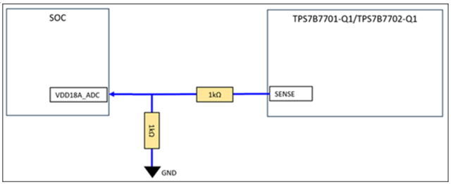
The SENSE pin of this IC is connected to the VDD18A_ADC of the SOC,

The valid detection value (max) for this pin (VDD18A_ADC) is 1.7V~1.8V~1.9V,

The pin withstand voltage is 2.5V.

Could you please confirm the following questions:

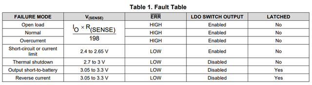
①、When the LDO switch output is disabled, is the output of SENSE a momentary high level, or will it continue to maintain a high level? (I am concerned it could cause damage to the subsequent stage)

(in cases of short circuit, current limit, thermal shutdown, etc.)

②、Is there any problem using the following circuit in the situation where issue ① occurs?

Thank you for your help.

  • Hi Zhao,

    (1) VSENSE will maintain a high level. When the LDO Switch is disabled due to thermal shutdown, short-to-battery, or reverse current, VSENSE is forced into a voltage range specific to its fault state. It basically doubles as an analog error flag. However, it should go to 0 when the EN pin is disabled.

    (2) Assuming the ADC is high impedance, those fault states can violate the pin max voltage of 2.5. The max it will force it to is 3.3V. As long as RSENSE is kept sufficiently low, you can regard this as the pin's upper limit. A voltage divider is the simplest solution, e.g.:

    Best,

    Gregory Thompson