This thread has been locked.

If you have a related question, please click the "Ask a related question" button in the top right corner. The newly created question will be automatically linked to this question.

UCC2803-EP: Start up circuit

Part Number: UCC2803-EP
Other Parts Discussed in Thread: UCC2803, , UCC2802

Tool/software:

Hello,

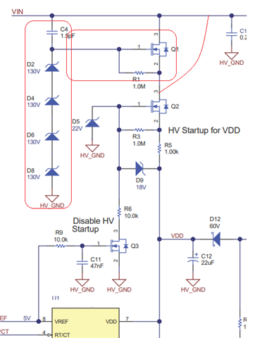
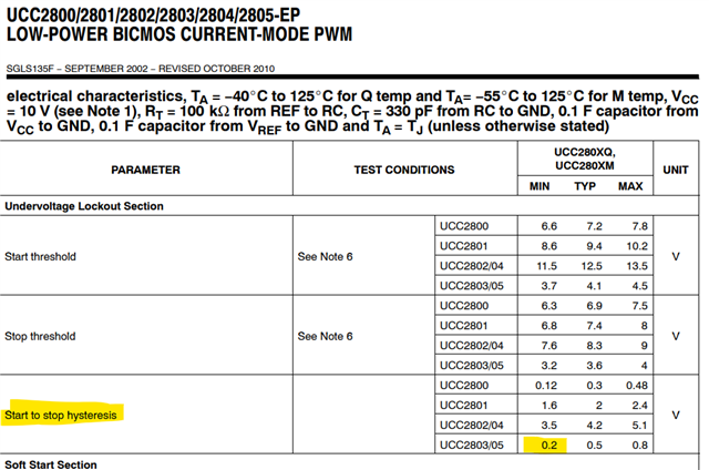
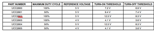
We are using UCC2803 Flyback controller IC.

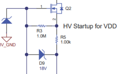
Regarding start up circuit , could you please help me a different approach apart from using resistor divider and charging the capacitor, time taken to charge the capacitor for UVLO would be more since we use high value of resistors.

Is there a different approach to eliminate this concern!

  • Hi,

    You can use a depletion FET such as BSS126 for up to 550V, and 2x BSS126 for up to 1000V input.

  • Hello,

    If we are using VREF to disable the HV Startup, but VAUX will be up after the softstart time. Then how do we power the UCC2803 until VAUX comes up?

    Are we using 22uF capacitor to do this? 

  • Hi,

    Yes, using 22uF stored energy to do this.

  • If R5 is used to limit the current , then wouldn't 1k be a very small value for high input voltage?

  • Hi,

    R5, R3 and D9 voltage have to be balanced. D9 VF = 0.3V (roughly), R3 cannot flow current to cause close to 2V when Q2 will be off then R5 has no current. If assume R3 voltage 1V, then R5 voltage can only be 1.3V, V(R5) = V(R3) + V(D9) = 1V +0.3V. So R5 = 1k is only allow 1.3mA current to flow no matter Vin is high or low, as long as BSS126 ok to sustain.

  • Hi,

    What would be the voltage at gate of Q2?

  • Hi,

    Q2 drain is Vin if you use one BSS126 and remove all red blocked. BSS126 Vds breakdown 600V.

  • Hi,

    How do we select the breakdown voltage of D9?

  • Hello,

    I understand D9 is to clamp the VGS voltage to its rated value when VDD coming externally exceeds its operating voltage. Please confirm if the understanding is right.

    But , D5 is required to clamp the VDD voltage which is charging the capacitor to its maximum value but the current which flows through it would be through 1Meg right , how will that current be sufficient to clamp the D5 Voltage?

  • Hi,

    Yes, D9 is to help clamp VGS < 20V which is abs max of BSS126.

    D5 is to help protection if Q3 is not turned on. Without D5 when Q3 is not on due to defect or damage, Q2 pin 1 becomes sort of floating then subsequent damage can happen from Q3 damage. After add D5, Q2 pin 1 is clamped at 22V so Q2 will be off when VDD reaches 24V so help avoid subsequent damages.

  • Hello,

    1. As per suggested BSS126, I have a query on power dissipation of mosfet.

    Current that flows through R5 is the current coming from the source of mosfet. Maximum input voltage in our case is 500V.

    So, Power dissipation of mosfet would be (500V)*(1.3mA) which is 0.65W and would be very high for this mosfet.

    Could you please provide your feedback on this.

    2. Also, as per UCC2803-EP datasheet i see start to stop hysteresis is 0.2V minimum. 

    If we consider this , then VCC Capacitor required to handle 0.2V drop for a startup of 10ms and 10mA VCC Current would be very high(~500uF).

    Could you please provide your feedback on this.

  • Could you please provide your feedback on this!

  • Hi,

    1., 

    Its SOA allows to flow 1.3mA at 500V for a quite time close to DC. In our design that time is about 200ms so ok. If your design also has similar time duration for 1.3mA then it is ok based on its SOA.

    2.,

    Not sure why you select UCC2803, but if that is a concern, then one possible is to use UCC2802 which has much large hysteresis. Or you add external circuit to extend the hysteresis. For example, you can delay to turn off Q2 until VCC reaches higher than 4.5V. It looks UCC2802 should be used in your case.


  • Hello,

    1. Drain current looks within SOA curve for 1.3mA , but how did we arrive at a value of Vth(Q1) is 1V as mentioned in your previous response?

    In the BSS126 datasheet i go get Vth(OFF) voltage varying from 1.6 to 2.7V. Could you please let know what value are we referring as 1V for calculating the current? Because we need to consider the range of Vth for calculating the maximum power dissipation.

    2. In our case we arent using VREF to turn off Q2 , we are using VAUX voltage to turn off Q1 , to be sure that once VAUX is up we are switching off Q2.

    Our scenario is UCC2803 turns on when capacitor charges to 3.7V since that is the minimum start threshold and as per hysteresis it turns off at 3.5V so we will have to store the energy in capacitor for 4ms(which is start up time). 

  • Hi,

    1.,

    We need to have about 1.3mA and at 1V, ID can be close to 4mA so BSS126 is ok to flow 1.3mA. Then we design external circuit with R3 and D9 to get this Vgs close to 1V, since if > 1V such as 1.5V, BSS126 will start to stop flow current so cannot get 1.5V, this overall 1.3mA keep flowing until VREF turns on Q3 or VDD > 23.5V.

    2.,

    Ok, you need to design external circuit to help with smaller VCC capacitors to deal with this device small hysteresis. 

  • Hello,

    Is there any reference that with 1Meg resistor across gate and source of BSS126 , VGS will result in 1V ?

    We are calculating the drain current keeping 1V as reference for 1k R3 resistor.

  • Hi,

    Voltage across R5 = Voltage (R3) + VF (D9), VF (D9) = 0.3V, then V(R3) = V(R5) - VF(D9), so when V(R5) > 1,3V, then V(R3) > 1V, Q2 is towards to off so lower current will be resulted through Q2 channel, but when V(R5) < 1.3V, then V(R3) < 1V, more current will flow through Q2 channel to cause more current flow through R5 to make V(R5) increase back to 1.3V. So select R5 = 1k can get roughly 1.3mA. 

    R3 = 1M is to help control the current at 1uA from 1V across R3 which current is also from Q2 channel. So if you use R3 < !M, then more current will flow through Q2 channel. We decide to use 1uA to make less losses.