This thread has been locked.

If you have a related question, please click the "Ask a related question" button in the top right corner. The newly created question will be automatically linked to this question.

TPS43061: TPS43061RTER

Part Number: TPS43061
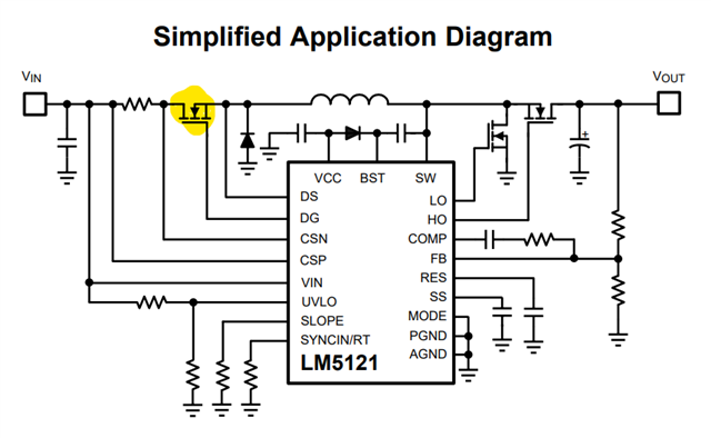
Other Parts Discussed in Thread: LM5121, LM5155, LM5122

Tool/software:

I am having a requirement for designing a Boost converter for charging a capacitor 200mF to 28V at a constant current of 2A From a 15V power supply 

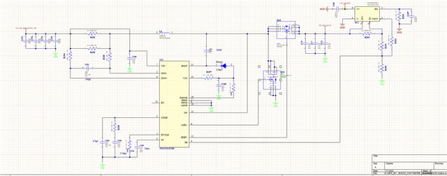
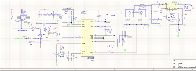
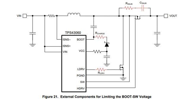
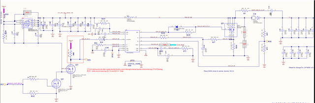
after checking in We-bench TPS43061RTER its suggesting this part number After checking this has input current limit but its not very precise can i Add an external current sense feed back control loop  to adjust Vfb ? Will this topology work ?

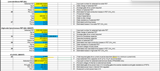
Sense Resistor (RSENSE)          
20 Vcs typ 0.070 0.071 0.071 V Typical over-current current sense voltage based on Figure 19 in datasheet
  Vcs min 0.057 0.057 0.061 V Minimum over-current current sense voltage (10 mV below typical)
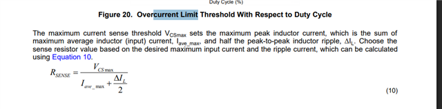
21 Rsense max 7.13E-3     Ω Maximum current sense resistor using Vcs min and 20% tolerance to account for efficiency and transients
  Rsense chosen 12.00E-3     Ω Selected sense resistor
22 P Rsense 0.560     W Minimum power rating for current sense resistor in normal operating conditions
  Ilim min 4.713 4.753 5.095 A Minimum current limit with selected sense resistor
  Ilim typ 5.848 5.890 5.928 A Typical current limit with selected sense resistor
  Estimated Efficiency 93% 96% 97%   Estimated Efficiency
  Iout max 1.908 2.133 2.493 A Maximum output current using minimum over-current sense voltage
  Iout max 2.436 2.717 2.955 A Maximum output current with typical over-current sense voltage

  • Hi Agxin,

    Thanks for using the e2e forum.
    You are correct about the TPS43061 device. It has overcurrent protection based on the inductor current, but it has no constant current regulation for the output integrated.
    Implementing an additional current loop that feeds into the FB pin is the right solution for this, so your implementation is okay.

    If you need some additional reference, here is an application note that focuses on the constant current loop.
    https://www.ti.com/lit/an/snvaa85/snvaa85.pdf

    Please let me know if you have any additional questions.
    Best regards,
    Niklas

  • Hi NIKLAS SCHWARZ ,

    Thanks for the response 

    I found one bug in my design there is a leakage path through the body diode of the top MOSFET, when the converter is off i will see a leakage and will create inrush to the supply ..

    so I have modified the design like this this is this ok will this gate drive capable to turn on two fets ?Do you see any mistake in the design ?

    To work for the below spec 

    Vin nom 15.2
    Vin min 14.9
    Vin max 16
    Viripple 0.152
    Vout 28.8
    Vripple 0.288
    Iout 2.125
    fsw 575

  • Hi Agxin,

    Thanks for the feedback.
    With this implementation, I am concerned about the Q13 MOSFT. Is it not about the driver strength, but about the orientation of the FET.
    I understand you want to block current from the supply to the output during off-time, but if you place a MOSFET like this, you might have problems during operation.
    For example, if you would have longer dead-times or a scenario where both LDRV and HDRV are turned off, the voltage at the switch node would spike as the inductor current has nowhere to go to. This would then damage the IC or the FETs due to overvoltage.

    If you want to avoid current running from supply to output during shutdown of the device, I would recommend to implement a disconnect circuit before the power stage instead.
    For example, we have the LM5121 device which uses a disconnect MOSFET for this exact purpose.

    Best regards,
    Niklas

  • Hi NIKLAS SCHWARZ ,

    Thanks for the valuable feedback

    But in the old schematics if I am not USING Q13 When Boost converter is not Enabled .. there is a leakage path , because of this I cannot completely disconnect the Top MOSFET ,in this case by Current limiter sense some over current during capacitor charging at the start , How does Q23 cut off it doesn't work at all .. the second loop that i have provided To monitor the output current and modify the VFB pin does't help because the Boost converter cannot cutt off the diode path any more till the output is higher than the input ..so during inrush it will create power trip

    Also in the below topology how does the current limit mechanism work at the start (during inrush ) , are there any smart ways to fitter the controller with more features like inrush limit etc 

  • Hi Agxin,

    By nature of the boost topology, you always have the direct connection from VIN to VOUT through the inductor and body diode of the high side FET.
    The strong inrush current when the supply is turned on cannot be avoided by the controller. (This will happen even if the controller is still in shutdown mode)
    The current limit function of the device does not apply here.

    The solution to avoid this inrush current and also allow full discharge of VOUT if the device is not active would be to fully cut the supply voltage through additional circuit, or change the topology.
    For this application, you can consider a SEPIC design with LM5155.
    SEPIC has no direct connection from VIN to VOUT, so you do not have the inrush current problem anymore.

    Best regards,
    Niklas

  • Hi NIKLAS SCHWARZ ,

    There are few Issues with this controller I am facing right now 

    when I use SEPIC topology 

    In fact my current boost in which i have problems with inrush

    This is the same part you are proposing for SEPIC topology .

    Even in the existing design if the converter supports higher say above 4 A i am ok to go with this part , Just i will modify it to SEPIC topology .

    But when i increase the current I am getting this phase margin too low for the compensation circuit  .Does we bench supports retuning the comp network ?

    how do i solve this ?

  • Will this doesn't help in such scenario ?

    How about adding a Diode in SW node ?

  • sorry to check with you on more questions 

    LM5121 if i go with this part for 7A ilim how do i calculate INRUSH2  when i feed my Vin MAX 15v The equation becomes negative  Are there any better explanation for this equation

  • Hi Agxin,

    Webench does not support tuning of the compensation by the user, so there are cases where a design is definitely feasible, but webench cannot suggest you a design.
    For such cases, I would recommend to use our quickstart calculator tool instead.
    https://www.ti.com/tool/download/SNVR481

    Another alternative is to look for reference designs. All the design shown here have been build and verified:
    https://www.ti.com/reference-designs/index.html#search?keyword=lm5155

    I also checked for SEPIC designs with synchronous controllers (high side MOSFET instead of diode).
    Here I found this design using LM5122, which should match your specification quite well:
    https://www.ti.com/tool/PMP31144

    Will this doesn't help in such scenario ?

    How about adding a Diode in SW node ?

    The dead-time is exactly the risk, because this is the time where both MOSFET are open and the inductor current is stuck.
    A diode will help in this case, but I have never seen such a implementation with two high side FETs facing each other, so I do not know if there are other risks we have not even considered yet.

    Best regards,
    Niklas

  • Thanks for the feedback

    This was the idea behind the additional mosfet 

    But for the inrush control using LM5121 can you clarify ?

  • Updated reference design 

  • Hi Agxin,

    Thanks for the clarification.
    So your idea was to implement an ideal diode controller to block the current path.
    This can indeed work, but I am not an expert on such circuits, so I cannot say if the most recent schematic with the capacitor between the FETs is sufficient or still needs further adjustment.

    To give more information on the LM5121 device,
    this device has an additional FET at the input side, which is turned off during shutdown to cut off the supply from the output.


    The effect is the same as the ideal diode controller approach, as you also disconnect supply and output with a MOSFET.

    Best regards,
    Niklas