Tool/software:
Hi all,
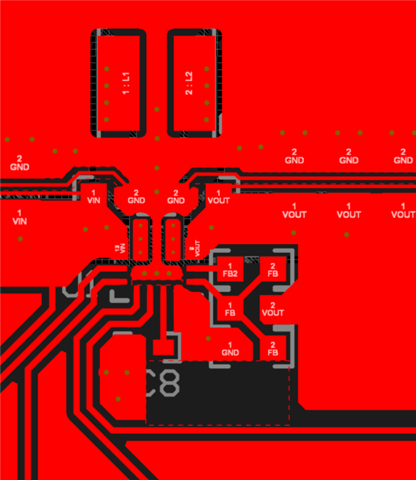
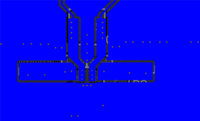
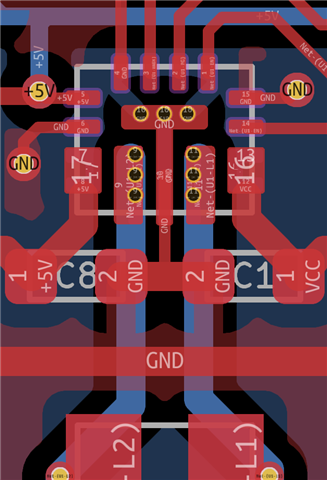
For a project I'm using TPS630701 fixed 5V output version, converting a battery input to 5V. Following the datasheet I have initially manufactured the pcbs with the layout in Figure 1 below. Recently while I was looking for the suggestions on power ground, I saw this suggestion: "Use a common ground node for power ground and a different one for control ground to minimize the effects of ground noise. Connect these ground nodes at any place close to one of the ground pin of the IC". I'm not sure if I've understood correctly but looking at the EVM layout, I've realised the ground pins are not connected underneath the IC. Therefore I've created a new layout, please see Figure 2. Could someone please comment if this is what is being recommended in the datasheet?
Figure 1: Layout 1, ground pins connected together underneath the IC
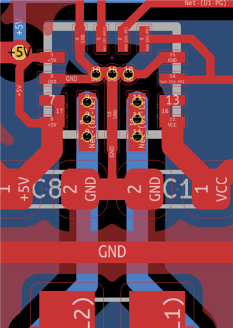
Figure 2: Layout 2, no ground connection underneath the IC, improved land pattern with solder max expansion for some of the pins.
My final question is: does this IC allow us to completely separate PGND and GND to fully isolate the circuit from the battery?
Many thanks,
Ersin