This thread has been locked.

If you have a related question, please click the "Ask a related question" button in the top right corner. The newly created question will be automatically linked to this question.

LM25037: LM25037 CS and Opto-emulator Feedback Layout

Part Number: LM25037

Tool/software:

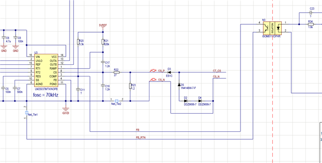
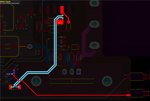
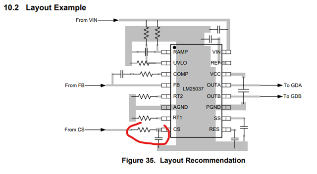
I’m designing a 12V–360V push-pull converter using the LM25037. The primary current is measured with a current transformer. Should the sense resistor be placed close to the CT transformer or close to the LM25037? Currently, the sense resistor is placed directly next to the LM25037. The CS_N pin is connected to the IC’s AGND. Also, should the emitter of the opto-emulator used for feedback be connected directly to the IC’s AGND as well? It is located about 4.5 cm away from the IC. Could you please provide some layout design advice?
The schematic and layout details are attached.

  • Hi,

    The sense resistor should be placed close to the current transformer. You can have another resistor close to the IC pins along with a small capacitor if you see noise after you use Kelvin connections like you show.

    Both opto and CT should use kelvin connections instead of using a copper plane for AGND.

  • Hi,

    Thank you for your response. Will it be a problem if the CS trace is a few centimeters long? I assume the CS input of the LM25037 is a high-impedance node, so it could easily pick up noise. Unfortunately, the MOSFET driver is located relatively close on the top layer. The CS trace will be routed on layer 3. Layer 2 is a GND plane, and layer 4 will also be GND. Do you have any recommendations for sizing the Kelvin trace? What impedance should I target for the CS Kelvin trace?

  • Hi,

    Yes, a few centimeters long is long. Yes, CS pin is high impedance, so the noise needs an RC filter while Rcs at CT spot helps limit the noise from CT locally and additional noise filtered out by RC.

    R can be 1k and C can be 47pF to 150pF