UCC27614: Drivers are still failing

Part Number: UCC27614
Other Parts Discussed in Thread: UCC27624, UCC57108

Tool/software:

Hi,

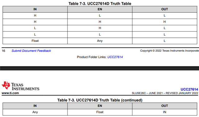
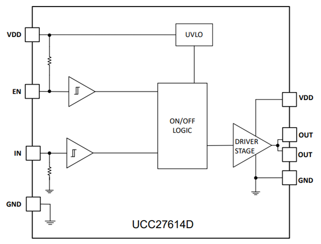
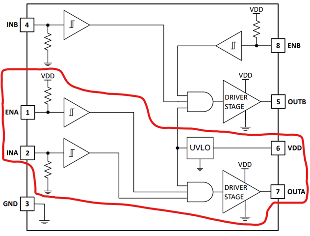
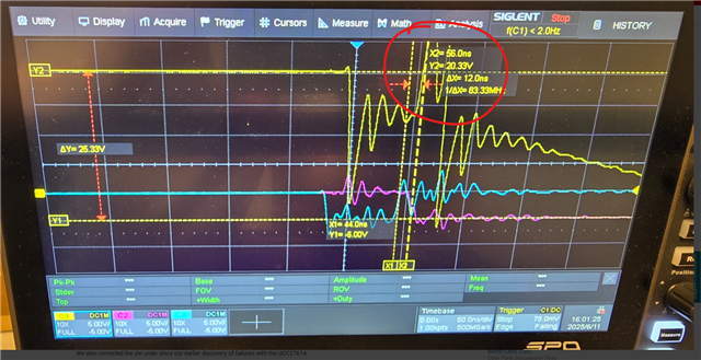
Following up on the previous discussion in this forum—we initially believed we had found a workaround for this issue. However, we've now observed that during switching events around 2000A at ~1000V, our current design occasionally triggers a brief glitch on the gate driver's input signal. This glitch, likely occurring within the same critical timing window as previously discussed, appears to cause permanent damage to the driver. The failure mode is identical to what we’ve seen before: no short on the OUT pins, but the driver stops functioning as if some internal logic or level shifter has been compromised.

Could you please confirm whether this issue has been addressed in upcoming batches? If not, we may need to explore alternative solutions and would welcome any recommendations.

Thanks in advance.

  • Hi Fredrik,

    Just to confirm, you are referring to this thread, correct?:  UCC27614: Destructive Overlap Between EN and IN+ Signals 

    To recap on that thread:

    1. You are pairing an external DESAT fault detection circuit with our UCC27614 (assuming the D package variant because you mentioned EN pin).

    2. Whenever the fault is triggered, the MCU pulls EN low to disable the driver. The EN goes back high after ~62ns.

    3. Because of ~75ns prop delay via isolators, IN remains high an additional 10-13ns after EN goes back high. This EN and IN high overlap damages the driver with VDD EOS.

    4. Your fix at the time was to increase the time EN is disabled to prevent overlapping.

    Please correct me if I'm wrong, but from the way I'm reading your understanding of the UCC27614 is that you believe when EN goes low, our driver has some delay until IN goes low. That is a common misunderstanding, and the main function of EN is to enable the output of the gate driver; EN status does not affect IN signal. The IC will process IN signal regardless of EN being high or low, but if EN is low, then the OUT will never go high.

    Here is a truth table of IN/EN/OUT:

    Here is a block diagram of UCC27614. Inside the "ON/OFF LOGIC" block, there's an AND gate that has IN, EN, and VDD UVLO as inputs. Once again, IN will be processed through the IC, but once it reaches the AND gate, it will check if EN is high or low, and it will go from there. I also attached the block diagram of the UCC27624, which shows a little bit more detail (the UCC27624 is basically the UCC27614 split into two channels):

    Your solution of increasing the delay of EN turning back on is good, but you need to also keep the IN signal in mind. This is the same for almost all other gate drivers.

    Let me know if this helped, or if you are experiencing a different issue; I can continue helping you out. You can also send me your schematic of the design, including the UCC27614, the isolators, and the DESAT circuit for preliminary analysis. Please also share the system characteristics, like the VDD, IN signal characteristics (PWM voltage, switching frequency, and duty cycle/pulse width), and EN characteristics.

    Also, just to put it out here, we have the UCC57108, which is a single-channel low-side driver with built-in DESAT detection system. If you're open to redesign or future projects, you can consider that device.

    Thanks,
    Rubas

  • Hi,

    We have tested this, and it appears that the issue is not limited to the previously discussed failure mode. In our application, we are switching at ~2000 A and +800 V, and when an arc develops in the plasma we are controlling, turning off the transistor via the gate driver can generate significant disturbances.

    If these disturbances couple into the signal path and momentarily turn the gate on for ~6–13 ns, the driver fails. This makes the current device unsuitable for our application, and we now need to consider alternative solutions.

    Have you specifically tested what happens if the gate driver is turned on for ~9 ns? If not, please investigate and either provide a revised driver solution or clearly state in the datasheet that the device cannot handle such transients.

    If you have alternative recommendations, please contact me via email. Possible candidates we are considering include UCC5880 or UCC5881. Our requirements are:

    • Output: –5 V to +20 V

    • Drive strength: 10–20 A

    • Maximum latency: 30 ns

    Thanks in advance for your support.

  • Hi Fredrik,

    If the disturbances that cause the gate to momentarily turn on results in high voltages exceeding the datasheet specs, then we cannot guarantee that the driver will survive. Can you clarify if this disturbance couples into the IN pins or OUT pins of the driver? Do you have waveforms showing VDD, IN, EN, and OUT voltages at the driver pins when the glitch/disturbance happens? Schematics would also be very helpful to analyze.

    Thanks,
    Rubas

  • I will not share schematics in this forum.
    The glitch is coupled into the IN pin.
    No, I dont have any waveforms to share. Its a very noisy environment, so its not possible to get a reliable measurement.
    We can easily kill it in a controlled way by just turning on with a short pulse, 6-13ns without having any gate resistor connected.

  • Hi Fredrik,

    We can move to email if you feel more comfortable sharing schematics/layout over email. Let me know if that's what you would like to do.

    It definitely looks like a noisy environment based on your waveform from the previous thread. I circled a potential spike on the gate that could potentially be exceeding our absolute max rating on the output pin:

    A noisy environment is very risky for the driver, so please ensure that all voltages at the pin of the gate driver is within datasheet specs.

    Thanks,
    Rubas