This thread has been locked.

If you have a related question, please click the "Ask a related question" button in the top right corner. The newly created question will be automatically linked to this question.

TPS2595: BPS topology – High current consumption when both EN = LOW

Part Number: TPS2595
Other Parts Discussed in Thread: TPS25948

Tool/software:

I'm facing a similar issue to the one reported in the following thread: TPS2595: High shutdown current observed while using the TPS259573 as a BPS. 

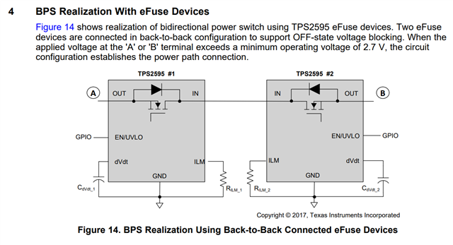
I’m implementing the BPS (Bidirectional Power Switch) configuration as shown in Application Note SLVA948 (Figure 14):
https://www.ti.com/lit/an/slva948/slva948.pdf


In my setup:

  • I'm applying 4 V at terminal A (OUT of the first TPS2595)

  • Terminal B (OUT of the second device) is left open

  • Both EN signals are held LOW (devices disabled)

However, I observe a current draw of ~10 mA from the first TPS2595, which is unexpected during shutdown. This causes noticeable heating of the IC even though it is supposed to be off. 

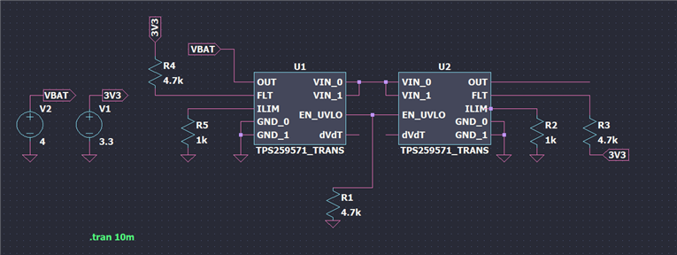
Below is a simplified schematic sketch of the implementation (note: I cannot share the full schematic at this time due to restrictions). The dv/dt capacitors are left OPEN.

Questions:

  1. Is this current expected due to internal leakage or ESD structures when OUT is supplied and EN = LOW?

  2. What is the recommended way to avoid this issue while still implementing a BPS topology using TPS2595?

The mentioned thread seems to be exactly the same issue I'm facing. Does anyone know how this thread was resolved or what the final conclusion was?

Thank you in advance.


  • Hi Paulo,

    I don't see any cap or res path to gnd at IN pins of these eFuse. You mentioned 10mA current flowing through the device, this can flow from OUT to IN via the body diode of device and go to some cap or res path to gnd at IN pin. The power dissipation in this case will be 10mA*~600mV = 6mW which should not cause too much heating.

    Just curious on why are you using this bi-directional power switch. Is it due to bi-directional current limiting or is it for reverse current blocking? What is the end application?

    It is difficult to check the final conclusion of that thread as it is 7 years old.

    Best regards,
    Arush

  • There are no CAPs or any connection in the IN pins. The application functions as a bidirectional switch that controls a battery. Due to its bidirectional nature, it can either connect a load (to discharge the battery) or a charger (to charge the battery)—in other words, it is a bidirectional switch managed by a microcontroller. The OUT pin of U2 is connected to either the load or the charger; however, a current of 10 mA is observed even when the circuit is open. When U1 is removed from the PCB, the current draw stops. Conversely, when U2 is removed, the current draw persists.

    For my application (battery powered), 10mA is quite relevant.

  • Hi Paulo,

    I understand that 10mA current is high in the battery powered application. If there is no path from IN to GND then there should be no leakage current but since you are seeing this, I am not sure on exactly what might be happening in your setup. 

    In general, I would recommend you use TPS25948. This device has an integrated back-to-back FET and RCBCTRL pin to allow bi-directional current flow or to disable it using reverse current blocking. The only benefit of using two eFuse in above configuration is if bi-directional current limiting is required. 

    Best Regards,
    Arush