This thread has been locked.

If you have a related question, please click the "Ask a related question" button in the top right corner. The newly created question will be automatically linked to this question.

TPS63060: Regarding Switching operation behavior

Part Number: TPS63060

Tool/software:

Hi support team all.
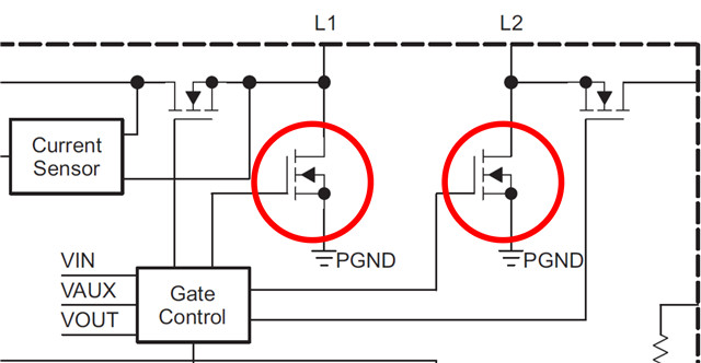
Switching behavior

Is it possible for both internal FETs in the diagram below to be turned on at the same time?
If so, under what conditions does this occur?
Currently, it has been confirmed that two FETs are turned on at the same time, which wastes energy in the inductor and prevents the output voltage from rising to the set voltage.

Best regards,

DH

  • Hi support team.

    I got the waveform date below.

    CH1:Vout

    CH2:L2

    CH3:L1

    CH4:Input current(before Cin)

    There is a period when CH2 and CH3 are both at GND.

    BR

    DH

  • Hi DH,

    Thank you for reaching out. What is Vin, Vout, Iout of the test? Can you also check inductor current waveforms? It seems that IC works in PFM mode, so it is normal behavior of skip phase.

    Regards,

    Mulin

  • Hi Mulin-san

    I share the additional information below.

    Vin=4V

    Vout=6V

    Iout=90mA

    I have an additional question.

    Is it really possible for two FETs to be ON when operating in PFM mode?

    The output is set to 6V, but it's dropping to 5V, causing the regulation accuracy to become very poor.

    It's unlikely that the regulation would be this bad when operating in PFM mode, so is this normal?

    Best regards,

    DH

  • Hi DH,

    I will reply to you later.

    Regards,

    Mulin

  • Hi Mulin-san

    I have some additional information from my customer.
    When this issue was confirmed, the board was two-layer, but the device's thermal pad did not have a thermal via and was not connected to the bottle layer directly below the device.

    After adding a thermal via to the thermal pad, the same device reported a change in operation. (The FET in the first quadrant was ON, the FET in the second quadrant was OFF, and output regulation returned to normal.)

    Based on these results, could you please tell me what the cause of this could be?
    This has caused customer evaluations to halt, and in the worst case scenario, we could lose business, so we would appreciate your help.

    Best regards,

    DH

  • Hi DH,

    Thank you for your patience and update. Can you ask customer to provide schematic and layout file?

    In the first waveform, Vout looks stable, but as you mentioned, Vout has 1V drop, I guess  there is something wrong, can you help provide the correct waveform?

    Regards,

    Mulin

  • Hello Mulin-san

    I have attached a waveform that shows it is working correctly.
    This was measured on a board with thermal vias added directly under the device.

    Also, I cannot disclose the circuit diagram and layout diagram in this post.
    I could send them by email. Is that possible?
    If that's OK, could you please let me know your email address?

    BR

    DH

  • Hi DH,

    Mu email address is mulin-yuan@ti.com. Please reach out to me and share me the design file.

    Regards,

    Mulin

  • Hi mulin-san

    Thank you for your email address.

    I sent you an email yesterday, so could you please check it?

    Best regards,

    DH

  • Hi DH,

    I have received the email. I will give you feedback in these two days.

    Regards,

    Mulin