


Tool/software:
Hello,
It looks like my earlier thread got locked due to inactivity. I still cannot get this circuit to charge a battery, despite a handful of hardware rework attempts and edits to the I2C configuration bytes. These serial debug messages are produced by the host microcontroller when a benchtop supply is turned on to apply a VAC input to this charger:
Charger interrupt triggered!
BQ25756E Register address 0x2B - writing value 0xE0
Status: CC Fast Charge
Power good = 1
Charge enabled = 1
EN_HIZ = 0
ADC conversion complete
Device entered Input Voltage regulation
Charge state transition
VBat = 11110 mV
VAC = 12054 mV
IBat = 0 uA
Iac = 0 uA
VFB = 1395 mV
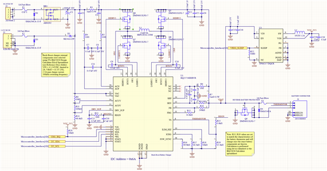
Here is my original, unmodified schematic:
So far, I have attempted the following fixes:
- Add thru-hole BAT41 Schottky diodes between DRV_SUP and each of the BTST nets
- Change R13 in my schematic to 0 Ohms to remove limitations on DRV_SUP current
- Change switching inductor to from 22uH to 10uH
- Put a 470uF electrolytic capacitor downstream of the input-side sense resistor to better balance capacitance
- Solder RC low-pass filters in parallel with the ICHG and ILIM_HIZ resistors
- Upon realizing that the STAT1, STAT2, and PG pins were directly connected to ground in my schematic, I disabled those pins via I2C write.
- Disabling ICHG and ILIM_HIZ pins via I2C write and replacing those resistors with 0-Ohm for full firmware control
- Since my present battery back does not have a thermistor, removed R15 and replaced R19 with 0 Ohms, then disable the TS pin via I2C write
Presently my firmware configures the IC as follows:
#define VAC_INPUT_MAX_mV 34000 //for VAC_DPM register
#define VAC_INPUT_MIN_mV 4500 //for VAC_DPM register USB charger with some voltage drop
#define IAC_INPUT_MAX_mA  1000 //for IAC_DPM register. 1A input limit seems fine. Technically we could set the limit higher whenever VAC is lower
#define MAX_CHARGE_LIMIT_mV 12600 //4.2V/cell * 3 cells
#define MAX_CHARGE_CURRENT_mA 2000 //pack is 2600mAh, so this is equivalent to 0.77C charge rate
#define CHARGE_TERMINATION_CUURRENT_mA 200// (MAX_CHARGE_CRRENT_mA/10)//In host-controlled applications, the termination current can be programmed using the ITERM register bits;
#define PRECHARGE_CURRENT_mA (MAX_CHARGE_CURRENT_mA/5) //charging current when battery voltage is above VBAT_SHORT but below VBAT_LOWV
#define VFB_REG_VOLTAGE_DESIRED_mV 1544 //set by hardware resistor configuration. Control loop tries to make voltage-divided charger output hit this target.
#define VFB_REG_OFFSET_mV 1504 //VFB when register is set to 0
#define VFB_REG_mV_PER_BIT 2
#define VFB_REG_VAL ((VFB_REG_VOLTAGE_DESIRED_mV - VFB_REG_OFFSET_mV)/VFB_REG_mV_PER_BIT)
#define VBAT_LOWV_LI_ION 0x3 //datasheet recommendation; 0x3 = 71.4% x VFB_REG; charger will only enter CC-fast-charge mode if battery is below 3V/cell; this is default value so we don't have to write
#define VRECHG_REG_VAL  0x3 //datasheet recommendation; 0x3 = 97.6% x VFB_REG; charger will top off battery once it drops below 4.1V/cell; this is default value so we don't have to write anything
#define ICHRG_REG_mA_PER_BIT 50
#define ICHRG_REG_VAL (MAX_CHARGE_CURRENT_mA / ICHRG_REG_mA_PER_BIT)
#define IAC_DPM_REG_mA_PER_BIT 50
#define IAC_DPM_REG_VAL (IAC_INPUT_MAX_mA / IAC_DPM_REG_mA_PER_BIT)
#define VAC_DPM_REG_mV_PER_BIT 20
#define VAC_DPM_REG_VAL (VAC_INPUT_MAX_mV / VAC_DPM_REG_mV_PER_BIT)
#define IPRECHG_REG_mA_PER_BIT 50
#define IPRECHG_REG_VAL (PRECHARGE_CURRENT_mA / IPRECHG_REG_mA_PER_BIT)
#define ITERM_REG_mA_PER_BIT 50
#define ITERM_REG_VAL (CHARGE_TERMINATION_CURRENT_mA / ITERM_REG_mA_PER_BIT)
#define BQ25756_TS_CHAG_BEHAVIOR_CTRL_DEFAULT 0x57 //power-on-reset value of the register
#define REG_TIMER_CTRL_DEFAULT 0x1D //power-on-reset value
#define DISABLE_ADC_DONE_INT (1<<7) //write to  REG0x28
#define DISABLE_WDT_INT (1<<3) //write to REG0x28
#define DISABLE_NTC_INT (1<<4) // REG0x29
#define BQ25756_ADC_CTRL_RESETVAL 0x60
#define BQ25756_ADC_CTRL2_RESETVAL 0x0A

#define EN_ADC_BIT (1<<7)
#define PART_ID 0x32
#define CHG_CTRL_RESETVAL 0xC9
#define CHG_EN_BIT 1
#define VFB_ADC_EN_MASK 0xFD
#define REG0x19_RSTVAL 0x20
#define DIS_PFM_MASK 0xDF

...

BQ25756_WriteReg(BQ25756_ADD, BQ25756_CHRG_V_LIM_LSB, (VFB_REG_VAL & 0x1F)); //charge voltage, bits 4:0 of register
    BQ25756_WriteReg(BQ25756_ADD, BQ25756_CHRG_I_LIM_LSB, ((ICHRG_REG_VAL << 2) & 0xFC)); //charge current, shifted and masked to fill bits 7:2 of first register
    BQ25756_WriteReg(BQ25756_ADD, BQ25756_CHRG_I_LIM_MSB, ((ICHRG_REG_VAL >> 6) & 0x07)); //charge current, shifted and masked to fill bits 2:0 of next register
    BQ25756_WriteReg(BQ25756_ADD, BQ25756_INPUT_I_DPM_LIM_LSB, ((IAC_DPM_REG_VAL << 2) & 0xFC)); //input current, shifted and masked to fill bits 7:2 of first register
    BQ25756_WriteReg(BQ25756_ADD, BQ25756_INPUT_I_DPM_LIM_MSB, ((IAC_DPM_REG_VAL >> 6) & 0x07)); //input current, shifted and masked to fill bits 2:0 of next register
    BQ25756_WriteReg(BQ25756_ADD, BQ25756_INPUT_V_DPM_LIM_LSB, ((VAC_DPM_REG_VAL << 2) & 0xFC)); //input voltage, shifted and masked to fill bits 7:2 of first register
    BQ25756_WriteReg(BQ25756_ADD, BQ25756_INPUT_V_DPM_LIM_MSB, ((VAC_DPM_REG_VAL >> 6) & 0x3F)); //input voltage, shifted and masked to fill bits 5:0 of next register
    BQ25756_WriteReg(BQ25756_ADD, BQ25756_PRECHRG_I_LIM_LSB, ((IPRECHG_REG_VAL << 2) & 0xFC)); //precharge current, shifted and masked to fill bits 7:2 of first register
    BQ25756_WriteReg(BQ25756_ADD, BQ25756_PRECHRG_I_LIM_MSB, ((IPRECHG_REG_VAL >> 6) & 0x03)); //precharge current, shifted and masked to fill bits 1:0 of next register
    BQ25756_WriteReg(BQ25756_ADD, BQ25756_TERM_I_LIM_LSB, ((ITERM_REG_VAL << 2) & 0xFC)); //precharge current, shifted and masked to fill bits 7:2 of first register
    BQ25756_WriteReg(BQ25756_ADD, BQ25756_TERM_I_LIM_MSB, ((ITERM_REG_VAL >> 6) & 0x03)); //precharge current, shifted and masked to fill bits 1:0 of next register

    //until we have a better-characterized battery with a known thermistor, let's disable the TS pin and JEITA charging to make behavior more predictable
    BQ25756_WriteReg(BQ25756_ADD, BQ25756_TS_CHAG_BEHAVIOR_CTRL, (BQ25756_TS_CHAG_BEHAVIOR_CTRL_DEFAULT & 0xFC)); //clear bits 1:0 to disable TS pin and JEITA

    //disable watchdog timer. We want to only intervene upon interrupt, so there should be extended periods without I2C traffic
    BQ25756_WriteReg(BQ25756_ADD, BQ25756_TIMER_CTRL, (REG_TIMER_CTRL_DEFAULT & 0xCF)); //clear bits 4 and 5 to disable watchdog

    //we don't want activity on the interrupt pin for any of these events (right now at least)
    BQ25756_WriteReg(BQ25756_ADD, BQ25756_CHRG_MSK_1, (DISABLE_ADC_DONE_INT | DISABLE_WDT_INT));
    BQ25756_WriteReg(BQ25756_ADD, BQ25756_CHRG_MSK_2, DISABLE_NTC_INT);

    //test: disable ICHG, ILIM_HIZ, PG and STAT pins
    BQ25756_WriteReg(BQ25756_ADD, BQ25756_PIN_CTRL, 0x30);

    //enable the ADC for a single conversion
    BQ25756_WriteReg(BQ25756_ADD, BQ25756_ADC_CTRL, (BQ25756_ADC_CTRL_RESETVAL | EN_ADC_BIT));
    BQ25756_WriteReg(BQ25756_ADD, BQ25756_ADC_CHANNEL_CTRL, (BQ25756_ADC_CTRL2_RESETVAL & VFB_ADC_EN_MASK));

    //disable PFM
    BQ25756_WriteReg(BQ25756_ADD, BQ25756_POW_AND_REV_CTRL, (REG0x19_RSTVAL & DIS_PFM_MASK));

    //charger should be enabled by default, but just in case:
    BQ25756_WriteReg(BQ25756_ADD, BQ25756_CHRG_CTRL, (CHG_CTRL_RESETVAL | CHG_EN_BIT)); //enable charger
After the initial register writes, the host microcontroller polls the registers for status in response to any activity on the interrupt pin, as well as periodically to monitor state of charge.
I have used similar TI parts in previous designs, but this one just refuses to work no matter what I try. Based on what you see above, is there something I'm missing?
