This thread has been locked.

If you have a related question, please click the "Ask a related question" button in the top right corner. The newly created question will be automatically linked to this question.

BQ25792: OTG use case

Part Number: BQ25792

Tool/software:

Hi Team,

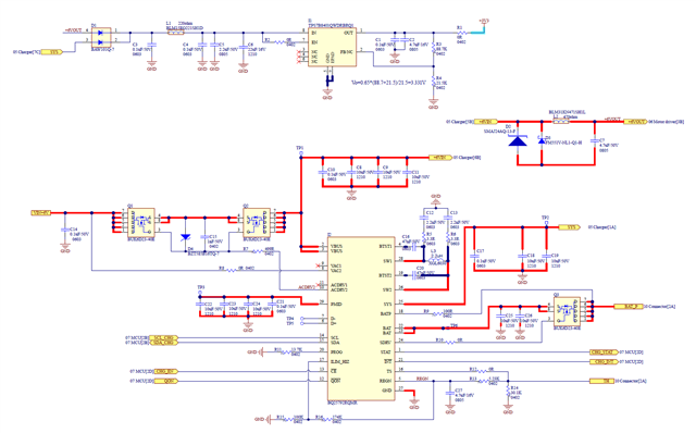
We plan to use OTG function on BQ25792. Below is the condition.

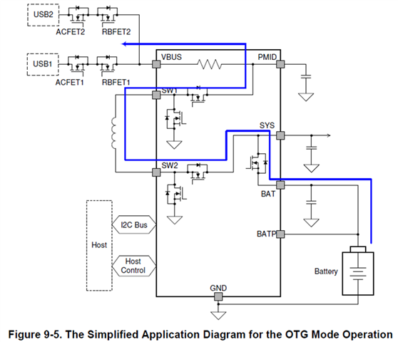
1. USB1 would be 5Vin when OTG doesn't work.

2. USB2 would be 5Vout when OTG work.

3. Battery is 1s architecture, around 3.7V.

My questions here are showing as below.

a. When USB1 work, the VBUS = 5Vin and Vsys would be around 3.7V, similar to BAT voltage that we set, charge voltage. Is it correct?

b. When USB2(OTG) work, we need to disable the EN_ACDRV1, enable EN_OTG and enable the EN_ACDRV, is it correct?

c. I would like to check if Vsys will have drop during the above transition? 

d. I would like to check if PMID will have drop during the above transition? If so, how can we estimate the drop time?

Regards,

Roy

  • Hi Roy,

    Regarding a, yes.  SYS is regulated slightly above charge voltage when charging.

    Regarding b, OTG on VAC2 cannot be enabled while there is a voltage on VAC1 because EN_ACDRV1 auto resets to 1 after the host sets it to 0. If VAC1 voltage drops below UVLO, EN_ACDRV1 auto sets to 0.  Then the host can write EN_OTG=1 and EN_ACDRV2=1.

    Regarding c, when both ACDRVx are off, the charger is in HiZ mode so the BATFET is turned on fully to connect BAT to SYS.  Worst case BAT could fall a diode drop below BAT.

    Regarding d, yes. PMID falls when VBUS voltage is removed. There are several 10s of milliseconds before OTG starts after the host writes EN_OTG=1 and EN_ACDRV2=1.

    Regards,

    Jeff

  • Hi Jeff,

    Thanks for clear comments. If we want to use OTG function, can we use VBUS2 only?

    May you help also review the circuit for us? Thank you.

    Regards,

    Roy

  • Hi Roy,

    The datasheet "Section 9.3.7.1 OTG Mode to Power External Devices" states the following:

    "For swapping the OTG output from port 1 to port 2, assuming EN_ACDRV2 is already 0, the host has to set EN_ACDRV1 = 0 to turn off ACFET1_RBFET1 first, which causes the converter to stop switching and VBUS to drop below VBUS_PRESENT. The host then sets EN_ACDRV2 = 1, and the converter starts switching again and ACDRV2 turns on ACFET2-RBFET2, which allows VBUS to ramp up. The similar procedure can be applied to the case of swapping the OTG output from port 2 to port 1."

    Following this procedure, you can use only port 2.

    I will let Jeff review the circuit when he returns to the office next week.

    Best regards,
    Michael