Tool/software:
Hi,
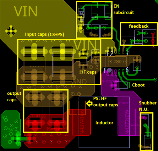
As a part of the Proof of Design I am performing on my custom HW, which utilizes LMR51440SDRRR to convert 24V to 5V,
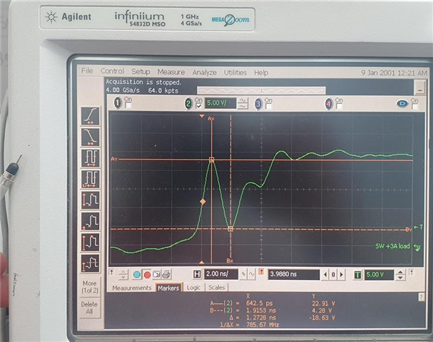
I measured the switching node between the LMR51440 and its inductor. The rising edge has a weird shape.
The voltage rises about 80% of Vin, then drops to 60% of Vin, then rises and finally reaches Vin (+minor overshoot). See image.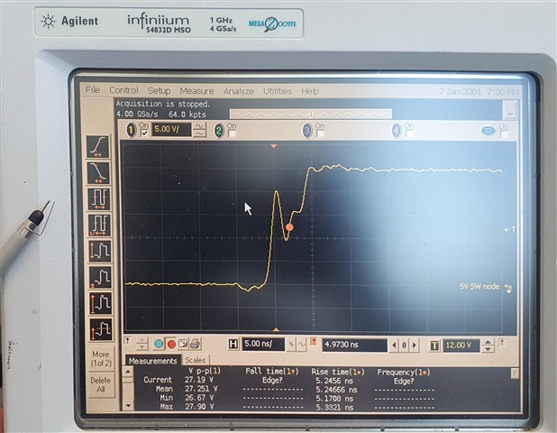
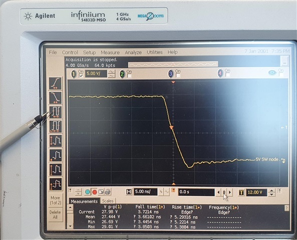
The falling edge does not show this phenomenon. See image.
Increasing the load on the buck output from ~0.6A to ~3.6A causes the peaks to grow farther apart (80% vin -> 90% vin, and 60% vin -> 20% vin).
Increasing the boot capacitor from 100nF does not make a visible difference.
Adding a series resistor (0.5 Ohm - 2.7 Ohm) to the boot capacitor reduces the first peak's value (2.7Ohm causes ~70% of vin), but does not change the overall shape.
Adding a snubber (100pF, which is as large as I can practically add regarding power dissipation) to the switch node increases both peaks voltage levels and causes an overshoot and ringing. It does not change the overall shape. It also adds ringing to the falling edge, which is unwanted because it looks fine.
I'll emphasize that this is not an issue by itself. The buck operates correctly, it is stable, and all is well.
I fear that, in the nearby future, when I take my custom HW to the lab to measure its radiated RF emissions, I will see it radiating strongly.
My questions are:
1. Does the EVM of the LMR514x0 show a similar weird shape on its switch node rising edge?
2. Do you have a theoretical explanation for this shape? For example something related to the high side switch driver method of operation, insufficient high frequency vin capacitors, etc.
3. Do you think this shape is just an artifact of my measurement setup? 1GHz scope, 500MHz probe, taken with a small GND spring as shown in image.
4. If you manage to recreate this on the EVM, do you consider this as an issue? If so, how do you propose to solve it?
Thank you.