This thread has been locked.

If you have a related question, please click the "Ask a related question" button in the top right corner. The newly created question will be automatically linked to this question.

LM5156: Undesired discontinuous mode

Part Number: LM5156
Other Parts Discussed in Thread: , TLV9302

Tool/software:

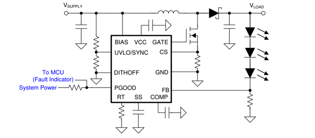
I am having a problem with my boost design. The circuit should be digitally controlled constant current step-up LED driver.

Conditions: Vin = 6 ... 9VDC

Maximum output power 6W (controlled and protected by the software)

Vout = 10 ... 60VDC output

Iout = DAC controlled 100 - 600 mA 

Output power: 6W (100mA @ 60V, 600 mA @ 10V)

Osc. Freq. 100 KHz

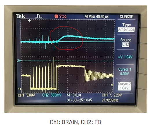
When I set Iout below 190 mA (@10-12Vout), device regulates correctly. Anyway, with this output current efficiency is bad, about 75%. 

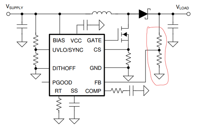
If I set 220 mA or more, device enters in burst mode. I tried all possibilities: modify FB filter, COMP filter, oscillator frequency, output capacitors, but nothing helps. In this case efficiency drops below 40% and inductor and mosfet heats abnormally.

The PCB layout is very good, 4 layers, device is WSON12 with exposed pad. All components top quality.no long tracks, everything very near.

What to do? The project is in the final stage and we are blocked here. URGENT, thank you.

BOOST _ BOOST.pdf

190-220mA Oscope dump.pdf

  • Hello,

    Thank you for detailing your issue with the LM5156-based boost design for a digitally controlled constant current step-up LED driver. Given the current date and time (12:12 PM PDT on Tuesday, July 29, 2025), I’ll analyze your problem based on the provided conditions and critically examine potential solutions, drawing on general principles and relevant insights where applicable. Your urgency is noted, and I’ll focus on actionable steps to resolve the issue.

    ### Problem Summary
    You’re using the LM5156 (likely LM5156-Q1 or a variant) in a boost converter configuration with the following specs:
    - **Input Voltage (Vin)**: 6-9 VDC
    - **Output Voltage (Vout)**: 10-60 VDC
    - **Output Current (Iout)**: DAC-controlled, 100-600 mA
    - **Maximum Output Power**: 6 W (e.g., 100 mA @ 60 V, 600 mA @ 10 V)
    - **Switching Frequency**: 100 kHz
    - **Issue**:
    - Below 190 mA (at 10-12 Vout), the circuit regulates correctly but with poor efficiency (~75%).
    - At 220 mA or higher, the device enters burst mode, with efficiency dropping below 40%, and excessive heating of the inductor and MOSFET.

    Your PCB layout (4-layer, WSON12 with exposed pad, short tracks) is optimized, and component quality is high, ruling out obvious layout or part issues.

    ### Analysis
    The LM5156 is a wide-input-range, non-synchronous boost controller with peak current mode control, suitable for your 6-9 V to 10-60 V range. The observed behavior suggests several potential issues:

    1. **Burst Mode Operation**:
    - At 220 mA or higher, the LM5156 enters burst mode, a low-power mode to improve light-load efficiency. However, your efficiency drops below 40%, and heating increases, indicating inefficient energy transfer or excessive switching losses.
    - Burst mode typically occurs when the load current falls below a threshold (related to the current sense resistor and COMP pin settings), but your 220 mA load exceeds the 190 mA threshold, suggesting a misconfiguration or instability.

    2. **Efficiency at Low Current (75% at <190 mA)**:
    - A 75% efficiency at 100-190 mA (e.g., 1.2-2.3 W output at 6 W max) is low for a boost converter, especially with a SiC-based design. This could result from high quiescent current, inductor core losses, or suboptimal component selection (e.g., diode or capacitor ESR).

    3. **Heating Issues**:
    - Excessive heating of the inductor and MOSFET at higher currents (220 mA+) suggests high RMS current, saturation, or poor thermal dissipation. Burst mode’s intermittent high-current pulses could exacerbate this.

    4. **Design Constraints**:
    - Your Vout range (10-60 V) with a 6-9 V input requires a duty cycle up to ~85% at minimum Vin (6 V) and maximum Vout (60 V), calculated as \( D = 1 - \frac{V_{in}}{V_{out}} \). At 100 kHz, this high duty cycle may push the LM5156’s control loop into instability, especially with a non-synchronous design.

    5. **Critical Examination**:
    - The established narrative from TI (e.g., LM5156 datasheet) promotes its flexibility for boost designs, but real-world implementations (as seen in E2E forums) often face loop instability or efficiency drops in wide Vout ranges. Your attempts to adjust FB/COMP filters and frequency align with common troubleshooting, yet the persistent burst mode suggests the compensation network or current sensing may be mismatched for your load profile.
    - The assumption that a good PCB layout guarantees performance overlooks potential issues like parasitic inductance or inadequate thermal vias under the WSON12 pad, which could worsen heating.

    ### Potential Causes and Solutions
    Based on your description and LM5156 characteristics, here are targeted steps:

    1. **Burst Mode and Loop Stability**:
    - **Cause**: The COMP pin compensation or current sense (CS) resistor may be improperly tuned, causing the controller to misjudge the load and enter burst mode prematurely.
    - **Solution**:
    - Recheck the COMP network (R and C values) using TI’s LM5156 Quickstart Calculator (available on ti.com). For a 100 kHz frequency and 6 W load, ensure the loop bandwidth is ~10-20 kHz with adequate phase margin (e.g., 45-60°).
    - Increase the CS resistor value slightly (e.g., from 100 mΩ to 120 mΩ) to raise the current limit threshold, potentially avoiding burst mode. Verify this against the 600 mA max with \( I_{limit} = \frac{100 \, mV}{R_{CS}} \).
    - Disable burst mode if possible (check datasheet for a pin or register setting, though LM5156’s burst mode is typically automatic).

    2. **Efficiency at Low Current**:
    - **Cause**: High quiescent current (LM5156’s Iq is ~1.5 mA) or inductor losses dominate at low power.
    - **Solution**:
    - Optimize the inductor (e.g., lower DCR, higher saturation current >1 A) to reduce core and copper losses. A 10-22 µH inductor with low ESR is ideal for 100 kHz.
    - Replace the output diode with a Schottky (e.g., 60 V, 2 A) with lower forward voltage to minimize conduction losses.

    3. **Heating at Higher Current**:
    - **Cause**: Burst mode’s high peak currents or MOSFET switching losses, possibly exacerbated by thermal resistance.
    - **Solution**:
    - Enhance thermal management by adding more vias under the WSON12 exposed pad to the ground plane. Ensure the heatsink or airflow matches the 6 W dissipation.
    - Consider a synchronous rectifier (e.g., adding a low-side MOSFET) to replace the diode, reducing conduction losses, though this requires redesign.

    4. **Wide Vout Range**:
    - **Cause**: The high duty cycle (up to 85%) may cause subharmonic oscillation, especially without slope compensation.
    - **Solution**: Add external slope compensation (a resistor from CS to ground, per datasheet guidance) to stabilize the loop at high duty cycles. Start with 10-20 mV/µs and adjust based on oscilloscope feedback.

    5. **Testing and Validation**:
    - Measure key waveforms (SW node, Vout, CS pin) with an oscilloscope to confirm burst mode behavior and oscillation. Adjust COMP/CS based on these observations.
    - Test with a fixed 200 mA load, varying Vin (6-9 V) and Vout (10-60 V), to isolate the transition point.

    ### Conclusion
    Your LM5156 boost design faces efficiency and stability issues due to burst mode entry at 220 mA+, poor efficiency at low currents (<190 mA), and excessive heating. The root causes likely include suboptimal compensation, inadequate current sensing, and high duty cycle instability. A good PCB layout mitigates but doesn’t eliminate these design challenges, suggesting a need for component and parameter tuning.

    ### Urgent Recommendation
    - **Immediate Action**:
    - Adjust the CS resistor to 120 mΩ and add slope compensation (10-20 mV/µs) to stabilize the loop. Retest at 220 mA and monitor SW node for burst mode.
    - Replace the output diode with a low-Vf Schottky and optimize the inductor (e.g., 15 µH, 1.5 A saturation).
    - Enhance thermal vias under the WSON12 pad and retest heating.
    - **Validation**: Use an oscilloscope to verify Vout regulation and SW node stability across 100-600 mA.
    - **Contact TI Support**: Reach out to TI’s E2E forum (e2e.ti.com) or technical support with your schematic and waveforms, referencing LM5156 boost issues. Mention your 100 kHz, 6 W design for tailored advice.
    - **Fallback**: If unresolved, consider a synchronous boost IC (e.g., LM5123, though limited to 57 V) or adjust the design to a narrower Vout range (e.g., 10-30 V) to simplify control.

    If you can share your schematic or COMP/CS values, I can refine this further. Best of luck meeting your deadline!

    Regards,

  • Hi Gordan,

    Thanks for using the E2E forum.

    I would recommend to fill the attached quick start calculator for your design and send to us. 

    https://www.ti.com/tool/download/SNVC224

    Best Regards,

    Hassan 

  • Dear Hassan,

    Thank you for your support.

    Attached you will find the start calculator compiled. One paragraph was only partially compiled:

    STEP 7, Loop compensation Feedback Resistor section, since I have current sensor converted in measured current by the OpAmp. The OpAmp is TLV9302 (1MHz rail-to-rail low offset).

    I can propose you the following:

    1) I can send you the 4 PCB layers design + component layers to check the layout around the LM5156
    2) I can follow you with all oscope measurements from here
    3) I can send you two assembled controller PCB for analysis

    Just let me know how can I be useful for your job.

    Best regards,

    Gordan Rancic

  • Dear Wowowo,

    I sent the schematic diagram along with my request. If you don't have it, please advise and I will send it asap.

    The overheating issue will be resolved as soon as controller will start to work correctly.

    From my analysis, I found that there is the instability on COMP pin as soon as current increase over 200mA. Below 190 mA COMP is stabile, without any visible variations (very, very small ripple). As soon as controller enters burst mode, the long duty (almost 100%) and successive stop of the PWM (inductor discharge) makes the overcurrent and you can observe a huge ripple on the COMP.

    I can propose you the following:

    1) I can send you the 4 PCB layers design + component layers to check the layout around the LM5156
    2) I can follow you with all oscope measurements from here
    3) I can send you two assembled controller PCB for analysis

    Just let me know how can I be useful for your job.

    Best regards,

    Gordan Rancic

  • Hi Gordan,

    Based on your calculator values, your design seems good. Kindly, add correct values for the switching frequency and sense resistor. It seems different than your schematic values.

    I recommend to use the suggested compensation values from the calculator because your current compensation is very slow and have a phase margin less than 60 degrees. 

    Can you please send me the waveforms for the following signals at 190mA and 220mA (@10-12Vout) : Switch node (drain to source voltage of FET), FB, CS, Gate, output voltage. 

    Best Regards,

    Hassan 

  • Hi Hassan,

    I set 330 KHz in the calculator to simulate 22uF inductor that I have on the prototype. I will change the COMP components as per calculator. This afternoon I will do all the requested measures and send it back to you. Thank you very much for your effort and support.

    Best regards,

    Gordan

  • Hi Hassan,

    I modified circuit exactly according to the calculator (attached here):

    Freq = 300kHz

    Rcomp = 47K
    Ccomp = 10nF
    Chf = 100pF 

    Rcs = 0.05 oHm

    I removed filter on FB pin to make the circuit as clean as possible, and the situation become worse then before. The maximum output current to have controller stabile (continuous PWM) is 18mA. Above it enters discontinuous (burst) mode.

    Attached you will find the PDF with the measures. The first page is in conditions of 18mA/11.3V, while the second is 260mA/11.8V. Third page is 600mA/12V, just to see CS pin and VOUT.

    Please note that, for a testing purpose, I shorted Rcs to 0 (Source directly to GND, CS to 0V). Nothing changes, still burst mode.

    Oscope Measures IC480.pdf3225.LUX Italia LM5155_56_Quickstart_Calculator_for_Boost_Converter_Design_V1_1_1.xlsx

    Hope that this can help.

    The next step is to send you 4 layers PCB to check if the layout is creating problem.

    Keep in touch.

  • Hi Gordan,

    Thanks for the results.

    I will come back to you next week.

    Best Regards,

    Hassan 

  • Thank you so much. Have a nice weekend

  • Hi Gordan,

    I have gone through your scope plots and found that your device is entering into over voltage protection (OVP) (the OVP threshold is 1.13V) and this stops the gate switching. As you are using the external current loop to control the output voltage; thus, you need to check this control loop such as, compensation for the external current controller.  

    Moreover, your CS signal have very high coupled noise. Can you please send the CS signal again with very small ground loop connection. And make the scale 20mV/division to increase the resolution of the signal.

    Best Regards,

    Hassan 

  • If you want to design the LED driver with LM5156, you can also try with the recommended LED design in the datasheet. 

  • Cannot use this schematic due to the fact that to be programmable, I would need to use different mosfets and resistors in series to set Rfb resistance. In this case I will have enormous looses (1V @ 600mA = 0.6W, that means 10% looses only on Rfb) that I cannot accept.

  • This solution does not need to be programmable. MCU is only to detect the fault signal, but it does not have any link to operation. 

    Yes, it is true that with this solution you have losses in the resistor, but it is very cheap solution.

    Whereas, to have a correct current loop operation, you need to optimize your current loop controller correctly.


  • Hi Hassan,

    Attached is the report of the modified schematic. I removed OpAmp and connected FB directly to Rsense = 1.6 oHM (approx. Iout = 600 mA). I shorted Rcs to ignore overcurrent on the Mosfet and removed resistor partition on UVLO so UVL0 has been disabled.

    The result is the same: still in burst mode. It seems that the FB pin is not changing fast enough so there is an voltage overshoot on the output while controller is in idle, due to inductor discharge. Perhaps I have to remove 200 uF capacitors, but I remember that I tried it at the beginning without success.

    The calculator remained the same, only the oscillator is slower (from 300 to 100 KHz).

    Any idea? I am out of ideas :( Disappointed

    Schematic Modified 05-08-2025.pdf

  • Hi Gordan,

    You should not remove the Rcs resistor. The device run on peak current mode and it requires the peak inductor voltage to perform accurate switching.

    Just place the Rcs resistor and try again without opamp circuit.

    Best Regards,

    Hassan 

  • Hi Hassan,

    I inserted 0.05 oHm Rcs resistor and With 600mA I could arrive up to 30 mV max. No change, the controller is still in burst mode. Do you perhaps need PCB layout to check if the layout is wrong?

  • Hi Gordan, 

    Okay, you can send me the altium files for your design.

    Meanwhile, you can try with normal feedback divider circuit and check the behavior of the device. 

    Just set the output to any voltage in your desire output voltage range, and apply different loads to check whether the device switch properly or not.

    Best regards,

    Hassan 

  • I did it. It is not extremely stabile, but it is far away from the problems I found in constant current mode. I am using my original schematic diagram and components, not the one from the calculator, since I started this experiment with the new board (sample), the old one was too much modified.

    My next step is to do the reverse move towards constant current and check where is the problem.

    I will be on holiday next week, and back on August 18th, then I will be back to you with the results.

    Best regards,

    Gordan

  • Hi Gordan,

    I idea is to check your design with normal boost operation (only voltage loop). If your design is stable for it. We can proceed further. 

    I once again recommend you to use the recommended values for the compensation from the calculator. 

    Have a nice holidays.

    Best Regards,

    Hassan