


Tool/software:
Dear TI Engineer,
Below is the schematic and layout of our design of BQ25710RSNR, can you help check if there any suggestion for the design?
Schematic is as below:
We designed a 10-layer PCB board, and the layout design details are shown as below:
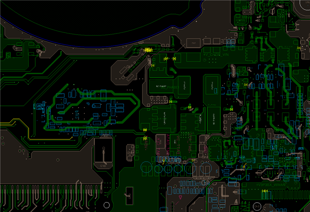
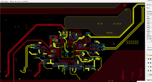
1) The top layer is as below:
2) Second layer is a complete GND.
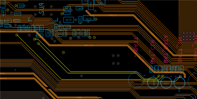
3) The third layer is as below:
4) The fourth layer is a complete GND.
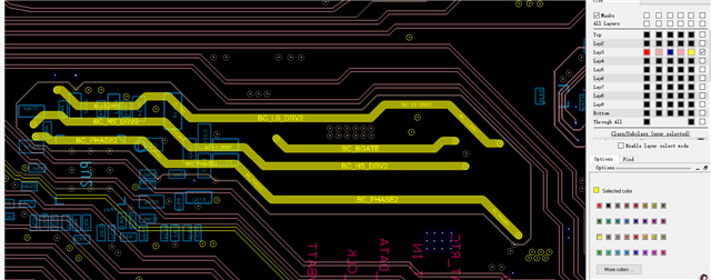
5) The fifth layer is as below:
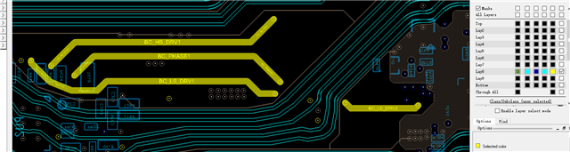
6) The eigth layer is as below:
7) The ninth layer is a complete GND.
8) The bot layer is as below:
Thanks,
Kind Regards
