This thread has been locked.

If you have a related question, please click the "Ask a related question" button in the top right corner. The newly created question will be automatically linked to this question.

TPS25730: PD configuration using the ADCVINx

Part Number: TPS25730

Tool/software:

Hi TI Team,

We are using the PD controller where we require a 12V (Min/Max) input with a 3A supply current.

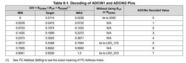
As per the datasheet, we have calculated the resistor divider values based on the ADCINx decoded value table (Table 8.1), which is attached below for your reference.

Could you please review the configuration and confirm if it meets the requirements for 12V@3A operation and FALUT_IN pin can be directly connected to the processor GPIO?

Please let us know if any additional information is needed.

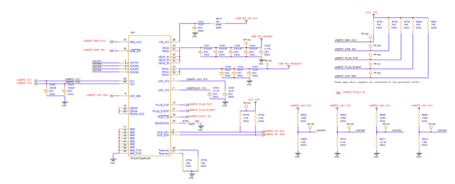
Additionally, I have attached the schematic for review.

Thanks & Regards,
Jaydip


12V 3A input     Pulled up at 3.3V ADC decoded value 
  ADC Input voltage  Rbottom Rtop  
ADCIN1  0.114671815 3.6K 100K 2
ADCIN2 0.160133206 5.1K 100K 3
ADCIN3 0.356199822 12.1K 100K 3
ADCIN4 0.058349705 1.8K 100K 1

  • Hello,

    Please be advised that the resistor decode in table 8-1 is the ratio between the upper and lower resistors and not the voltage at the ADCIN pin.  So for example, Rbottom = 3.6K and Rtop = 100K results in a resistor ratio of 0.035 (3.6K/(3.6K+100K)) and a decoded value of '1' - not '2'.

    FALUT_IN pin can be directly connected to the processor GPIO

    /FAULT_IN is active low, while you can connect the pin directly to the processor GPIO it may be a better system solution to use a pullup and then the processor GPIO would pull the signal low in the event of a fault.  IE what do you want the state of the /FAULT_IN while the processor is booting.

    Regards,
    Chris

  • Hi Chris,

    Thank you for highlighting the ratio-decoded value calculations.

    Based on the provided formula, I’ve updated the table to align with our requirements, where we need 5V/12V input at 0.5A–3A capacity.
    Please find the updated table attached for your review.

    As the processor will be powered by this PD controller, I believe the /FAULT_IN pin should remain high by default, and we will include a pull-up resistor to ensure this.

    Additionally, I plan to connect the other open-drain outputs to the processor GPIOs as outlined in the reference schematic.

    Please let me know if any further modifications are needed.

    Q2. Above Table 8.1 it is mentioned that decoded value for ADCIN1 and ADCIN2 but it is actually for ADCIN1 to ADCIN4 right?   

    Q3. As Processor IO voltage is 1.8V so we have applied the External VCC_1V8 to all the open-drain output instead of PD's internal 3V3 LDO, does FAULT IN pin supports 1.8V logic?  

    5 or 12V @0.5-3A input requirement       ADC decoded value 
      ADC Input ratio Rbottom Rtop  
    ADCIN1  0.015748 1.6K 100K 0
    ADCIN2 0.180328 22K 100K 3
    ADCIN3 0.015748 1.6K 100K 0
    ADCIN4 0.5 100K 100K 5

    Best regards,
    Jaydip

  • Hello,

    Please find the updated table attached for your review.

    Yes.  The updated values look good.

    Q2. Above Table 8.1 it is mentioned that decoded value for ADCIN1 and ADCIN2 but it is actually for ADCIN1 to ADCIN4 right?   

    Correct.  ADCIN1 to ADCIN4. I have submitted a request to update the document.

    Q3. As Processor IO voltage is 1.8V so we have applied the External VCC_1V8 to all the open-drain output instead of PD's internal 3V3 LDO, does FAULT IN pin supports 1.8V logic?  

    Yes.  1.8V logic will work.  Please see Vih and Vil for the TPS25730; 1.3V and 0.54V respectively. https://www.ti.com/lit/ds/symlink/tps25730.pdf#page=17

    Regards,

    Chris

  • Hi Chris,

    Thank you for addressing all the queries.

    Regards,

    Jaydip