BQ25308: BQ25308 fails when connected to AC/DC wall adapter 12V charger.

Part Number: BQ25308

Tool/software:

Greetings,

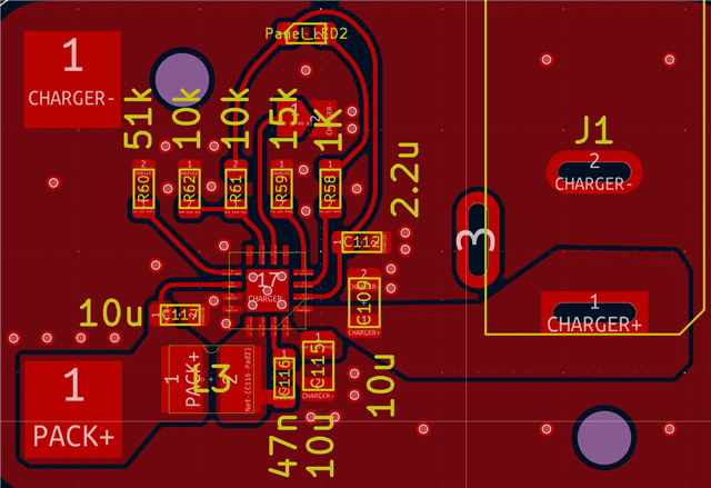
I have made the BQ25308 charger for my 1s Li ion cells at 2.6A charging current. It has worked when testing over a benchtop power supply. But when its connected to a generic AC/DC 12 volt 2A wall adapter like those used for wifi modems the charger has failed multiple times. Its indicator led also stops. When I replace the IC the circuit works again when testing with a benchtop supply. Please let me know what is causing this issue and mitigation steps. I have attached the schematics and layout of my charging circuit and an image of a generic charger. This is urgent as the device in customer's hand.

Note: I have noticed that this failure occurred when I switched on the AC/DC when it was connected to the IC. Could this be due to spike in voltage at startup of the AC/DC converter? 

Best regards,
Rasool


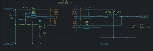
Charger layout.pdfibom.html

  • Hi Mohammad, the only variation from our recommended schematics I can see is the 10uF capacitor on VBUS. We typically recommend 2.2uF, and that any additional capacitance be placed on PMID. However this is unlikely to be the cause of the issue.

    Could you capture a wave form of the VBUS, and VSYS voltages, as the adapter is plugged in. I will also consult with some of my co-workers to see if they have ever seen issues with these types of adapters, however I personally have not.

    The part should be tolerant of 28V on the VBUS pin so it would have to be quite a large spike, however if this is the case I would recommend the addition of some type of protection like a TVS diode.

  • Thanks, Samuel, for the reply. I had a consultation with an engineer regarding this issue this morning. I had a Zener diode (1SMB5929BT3G) readily available, so I placed it at the IC inputs in the schematics. This is what he had to say:

    "I think it is not overvoltage problem. The chip can handle 28V. My best guess is a RACE condition between the two converters. When the ACDC voltage is not ramped up yet, the battery charger turns on with 2.6A output current, and hits the current limit of the ACDC converter, which turns off, and the long cables make a large negative voltage transient that will go through the ESD protection structure of the BQ25308 damaging it and creating permanent short-circuit inside the chip. The Zener diode you placed is not characterized in the forward direction, and other zeners I checked have high forward current drop. My suggestion is to place a high current Schottky diode in parallel to the zener diode to bypass the BQ25308 internal ESD structure in case of reverse voltages."

    Currently, I do not have access to the ac/dc I am at the site.

  • That certainly could be the issue however, assuming the cell is at ~3.6V and charging at 2.6A that would likely draw a current of less than an amp. In addition if the voltage source begins to crash, the charger has the VINDPM feature that will limit the charge current to prevent crashing the voltage source, this is particularly useful in cheaper and long cables with high impedance. It is outlined in section 9.3.4.1.2 of the datasheet. If the adapter is simply turning off due to a protection circuit VINDPM would not help but if it is "crashing" due to over draw VINDPM should prevent this.

  • They say that the AC/DC is fine at 12V but the charging has stopped. Currently I can only replace the ic and connect an already ON AC/DC to charge. I have tested and this way I thought ic would not face any startup transients. 

    Apart for the ESD and reverting to 2.2uF at Vbus, do you recommend any additional improvements/precautions.

  • There is nothing particular I can recommend right now, the best thing would be to capture some waveforms, of the adapter being plugged in. If you would like to send the device's PCB layout I can also review that.

  • Here is the attachment of the pcb layout.
    1205.Charger layout.pdf

  • Hi Mohammad, I don't see any glaring issues although it is a bit difficult to tell much from these raw outputs, especially without part markings.

  • Here it is. All the routing is on first layer and solid gnd underneath. All the vias are connected to ground.

  • Routing Looks good, when the chip is fried using the 12V adapters, is there a unexpected short created between any pairs of pins, VBUS and GND, or  VSYS and ground?

  • Yes, Vbus to gnd.

  • Hi Mohammad, the most likely thing to cause that in my opinion is a large voltage transient on VBUS, have you tried this with any other adapter types or just the one adapter?

  • Hi,


    There's no update for a while. The thread is considered resolved and closed.


    Thanks,


    Ning