UC1842: UC1842 and UC1842A

Part Number: UC1842

Tool/software:

I have got few questions about UC1842 and UC1842A.

1) Can we design the power supply without opto- isolator using these ICs?

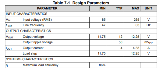
2) Shall I use my test requirement voltages in calculations or operating voltages in calculations, for example I am designing a power supply with Vin of 115+/- 10% as my input operating voltage, and power supply testing requirements are 115+/- 20%

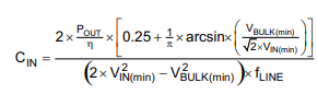
3) Equations for Vin ripple and Cin are same in UC1842A datasheet, which one is correct?

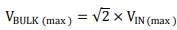
4)  How do we calculate Vbulk (min ) and Vbulk (max)? In one datasheet Vbulk (min ) is 95V and in other it is 75V.

5) In UC1842 Datasheet page 25, equation 18., how do we calculate Lm?

6) In UC1842 EQUATION 39, What is Mideal? Is it same as Mc? Mc can't be found until I know Se and Sn according to equation 38. To find Se I need Mc according to equation 41.

7) Why the simulation on Webench for 12V SUPPLY With same specification as in application note gives me different Nps and Npa values as compared to datasheets?

8) How can I design EMI filter for power supply to pass DEF STAN 59-411 and Mil-STAN-461 EMC

  • Hi Sumaira,

    Thank you so much for reaching out. Please give us a few days, and we will get back to you with the answers! Thank you so much for understanding.

    Best,

    Adhvaidh

  • Hi Sumaira,

    Thank you for your patience and understanding. 

    1) It depends on the converter that your using. If it is a non-isolated converter, then, yes, you can design your system without the opto-coupler. But, if it is an isolated converter, then optocouplers are required, as it is used to send error signal across the isolation barrier. 

    2) Can you please explain what you exactly mean by test requirement.

    3) Thanks for noticing. Only the equation for Cin is correct.   

    4) V_Bulk(max) is calulated using this formula:  . The, V_bulk(min) depends on C_IN.  Usually it is sized from 100-200uF.

    5) The value for Lm is based on the transformer you choose. Usually, it is around 3% of the primary inductance.

    6) In peak current mode control, we want the sub-harmonic oscillations to die-out within one switching cycle (So we want Q_p to be 1). Yes, M_ideal is a special case of M_c where Q_p is 1. You would first select a Q_p value, we get M_c. Based on the selection, we get the required slope compensation (S_e)

    7) Could you please share your webench link, I will look into it and get back you.

    8) Usually, differential mode filter and common mode filter are used. I found some links online for the military and defense standards.  https://www.vptpower.com/resources/videos/mil-std-461-conducted-emissions

    https://www.kamic.se/uploads/products/categoryfiles/Military-Vehicle-Filters-KAMIC.pdf

    https://premieremc.com/process-for-selecting-an-emi-filter/

    Hope this helps.

    Please let me know if you have more questions.

    Thank you.

    Best regards,

    Adhvaidh 

  • Hi Adhvaidh, 

    Thanks for your reply. 

     1)  The Normal operating conditions of power supply that I am designing is 115V+/- 10% but it will be tested at 115V+/- 20% in order to comply with MIL-STD-1399-300 test. i.e. Voltage and frequency transient tolerance test. 'The EUT performance shall be evaluated under the transient frequency and voltage conditions (from nominal) specified in table. Frequency testing can be accomplished on a component basis in lieu of larger modules or complete unit testing. This test shall be performed at normal operating load.' It will also be tested for Overvoltage condition of 150V for 24 Hours. In this case shall I design it for 115-20% to 150V AC?

    2) How Vbulk(min) will be dependant on C-in? What is formula to calculate  Vbulk(min) from value of Cin?

    3) My webench link is: 

    https://webench.ti.com/appinfo/webench/scripts/SDP.cgi?ID=63A331A7465D954D

    4) Does Simulation model provide for LT spice works for this design. I am using the un-encrypted version to simulate the design. I am having some issues to make it work. 

    5) Shall i select Qp value to be 1 for calculations?

    6) There isn't much in datasheet about Transformer specification calculation. Is there any other reference material that I can use for Transformer design?

  • Hi Sumaira,

    Thanks for reaching out again!

    1) Yes, in that case, you can design it for 115 V +/- 20%.

    2) You can plug in the Cin value into the same formula and solve for Vin bulk


    3) I have updated the operating conditions based on the design parameters table given in UC1842A datasheet (Page 15, Table 7.1). Now it matches the Nps value given on the datasheet. Please refer to the updated Webench link: https://webench.ti.com/appinfo/webench/scripts/SDP.cgi?ID=90E155D6B74DC2CD

    4) Please give me some time on this question. I will look into it and get back to you.

    5) If your application requires you to use a Qp of 1, then yes!

    6) Yes, please refer to this applications note on inductor design for flyback. 

    Thanks,

    Best regards,

    Adhvaidh

  • Hi, 

    Thanks for your reply.

    What does Qp specifies and how do I get it from my requirements?

    The document about the transformer only shows primary and secondary winding calculations, My design has got Auxiliary windings as well. How do I do calculations for that. 

    Regards, 

    Sumaira

  • Hi Sumaira,

    1) In peak current mode control, when you operate your converter at D>0.5, sub-harmonic oscillations can be observed for N number of cycles, and we use slope compensation to avoid it. Now, the quality co-efficient is the characteristic equation of the converter's double pole at half the switching frequency. The Qp value determines how damped the system's double pole is. Ideally, we want to damp the pole and stabilize the control loop without overcompensating (corresponds to Qp = 1).

    2) You can use this equation to design your Aux winding:


    Thanks,

    Best,

    Adhvaidh

  • Hi Adhvaidh, 

    Thanks for your reply. Can you please have a look at this simulation: 

    webench.ti.com/.../SDP.cgi

    Cin in this simulation is 10.8uF, In your previous replies you mentioned it should be between 100 and 200uF. Do you know why am i getting 10.8uF in simulation?

    Also in UC1842 datasheet I can't match calculated Rvcc value to simulation. Equation 5 on page 13. Can you please explain how to calculate that?

    Ipk (diode) that I have calculated using formulas in UC1842 datasheet (Equation 18, 19, 20) is 9.42A. The output diode selected in simulation is SS24FL. SS24FL can have average rectified current of 2A, which won't b enough. 

    I have taken Lm= 3% of Lp. Calculated Lp= 50mH

    Cout also different from simulation result. In simulation it is 180uF. For Iout of 0.676mA, I get Cout around 1500uF.

  • Sure!

    Could you please re-paste the Webench link? It's not accessible.

    Thanks,

    Best,

    Adhvaidh 

  • Hi, 

    Following is link to design.

    Vin= 85V to 160V (AC)

    Vout= 5V

    Typ Current= 0.517A

    Max. Current= 0.676A

    https://webench.ti.com/appinfo/webench/scripts/SDP.cgi?ID=E55849DFAD498847

  • Hi,

    1) Having Cin between 100-200 uF, is just a starting point in most designs, and not a necessity. 

    2) What is the calculated value of R_vcc(max)? The equation (5) is the maximum resistance value that you can select by still maintaining low input impedance at VCC pin. If your calculated value is within the calculated value, you should be fine. 

    3) The average diode current is the total output current (0.67 A), and not equal to the peak current. The output diode peak current is just the MOSFET peak current reflected to the secondary side. For this diode, the peak forward surge current is 50 A! Also, we have 2 diodes in parallel, so it should be fine. If you are implementing it in hardware, I would recommend you use a part with I_F > 5 A, instead.

    4) Could you please confirm if you are using 98.8 kHz as the switching frequency in all your calculations?

  • Hi, 

    2) R_vcc is referenced as Raux in simulation and is 10 Ohms. I have calculated is using following formulas: 

    If using 2N6802 transistor.

    Qg of 2N6802 or equivalent is 4.46nC

    Ioutput =4.46n x 50.58kHz = 0.023mA

    Vin (min) is voltage that will be available for IC:

    For minimum input voltage i.e. 85V, Vin(min) for IC is:

    = Vin (peak)- Vripple/2-Diodes drop

    Vin(peak)= 120.21

    Vripple is usually 15% = 120.21x0.15 = 18.03V

    Two diode drops = 0.6 x 2 = 1.2V

    Vin (min) for IC = 120.21- 9.01-1.2 = 109.99V

    Vvcc (max) = maximum voltage of IC= 30V

    Using formula on page 13, equation no 5:

    Rvcc (max)= 109.99 – 30/0.011 +0.023m = 2352.6=2.35k Ohms

    This value is lot higher than 10 Ohms

    I have used Ivcc= 11mA

    Iouput recommended is 200mA from datasheet but I have calculated based on formula on page 13, equation 4 for specific Transistor. 

    I am not sure why I am getting big difference in values?

    4) I am using 50.588KHz as switching frequency. Following is simulation link:

    webench.ti.com/.../SDP.cgi

    3) What should be Rramp and Rcsf?

    4) Did you get a chance to look at Spice Model of this device, It doesn't work for me on LT Spice.

    Regards, 

    Sumaira

  • Hi Sumaira,

    - Vin (min) is the minimum voltage that is used to supply VCC. VCC here is supplied by the auxiliary winding. Please use the voltage across the auxiliary winding. Also, the Qg of the MOSFET is 33 nC, and not 4.46 nC. From the datasheet "In normal operation, power VCC through a current-limiting resistor. Although quiescent VCC current is only 0.5 mA, the total supply current is higher, depending on the OUTPUT current. Total VCC current is the sum of quiescent VCC current and the average OUTPUT current." Hence, total VCC current would be (0.5 mA + I_OUTPUT) = 2.1 mA.

    Since your IOUTPUT is within the recommended value (200 mA), you should be fine.

    - The simulation link is not accessible. Could you please re-send it? 

    - R_ramp, and R_csf depends on the compensation slope. Please refer to the datasheet (pg. 29)

    - Please give me some time, I will look into the SPICE model and get back to you. 

    Thanks,

    Best,

    Adhvaidh