Other Parts Discussed in Thread: LM5171
Tool/software:
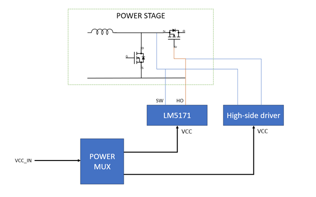
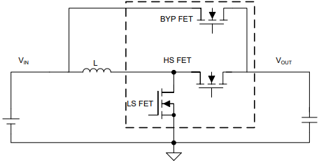
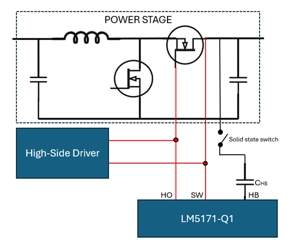
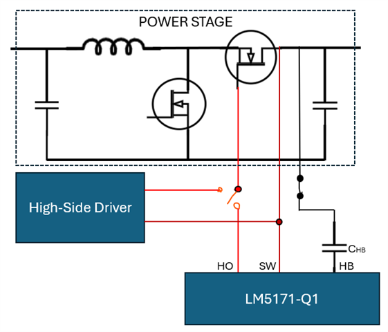
We are designing a topology as shown in the figure. To have a bypass mode where the power stage itself is used as the bypass path, another high side driver output that supports 100% duty cycle is, tied together with the LM5171 gate driver outputs. It is made sure that only one of the IC is powered ON at a time by using a power multiplexer configuration to supply the VCC to the IC's. Is there any risks involved in this topology or am i good to go? (PS:It will be made sure that there is no time when both will be in ON condition by providing sufficient delay).