This thread has been locked.

If you have a related question, please click the "Ask a related question" button in the top right corner. The newly created question will be automatically linked to this question.

LM5143-Q1: LM5143QRHARQ1 Design pcb

Part Number: LM5143-Q1

Tool/software:

Dears

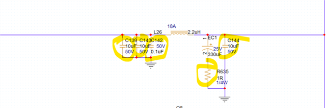
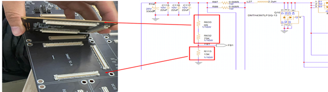
         1,By installing different daughter boards, adapt to different voltage requirements. As shown in the figure below, R633 and R632 are installed on the daughter board, and R113 is installed on the bottom board. When the two boards are assembled together, the required voltage is achieved. Can this method be used for design

           2,Can you provide a calculation table to inquire about the maximum current that LM5143Q can withstand in its current design?

  • Hello Honle,

    The feedback resistors are typically placed near the controller FB pin, as it's important to keep the FB trace short (it's a high-impedance node susceptible to noise). The proposed strategy seems feasible if the FB trace is purposely kept minimum length and surrounded by GND plane.

    Maximum output current depends more on the power stage components, max ambient temperature, airflow, etc. You can use the quickstart calculator to check component power losses.

    Regards,

    Tim

  • Dears

            Replace the input ceramic capacitor's withstand voltage value with 50V and increase the ground resistance by 1 Ω,it is ok?

  • What is the Vin-max spec here? I notice the damping cap is only rated to 25V. Btw, the ESR is the damping cap is likely sufficient. Rdamp = SQRT(Lin/Cin), where Cin is the derated ceramic value.

    10uF/50V ceramic is fine.

    Regards,

    Tim