UCC28180: Soft Startup failure

Part Number: UCC28180

Tool/software:

Dear TI Mentors,

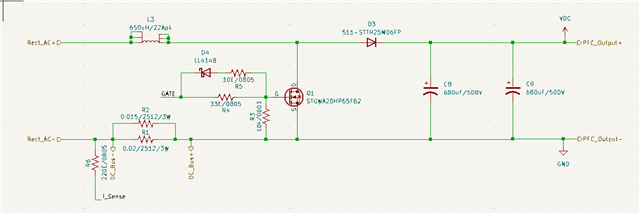
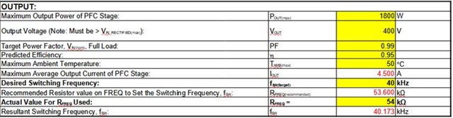
I have designed a Boost PFC stage using the UCC28180 (8-pin) controller, targeting a maximum power rating of 1.8 kW. All component values were calculated using the TI-provided worksheet. This PFC is intended for use in a motor controller application. At this stage, I am evaluating the Boost PFC section independently to verify that it can deliver up to 1.5 kW (nominal).

Test Setup:

  • Input: AC supply, gradually increased up to 175 VAC

  • Output: Connected to the bulk capacitor (no load connected yet)

  • VCC Supply to UCC28180: Provided externally via a DC constant voltage source (CV) turned ON after reaching the the stable DC voltage  — (later to be replaced with a flyback buck converter in the final design)

DC Bus Behavior:

     Upon ramping the input AC to 175 VAC, the DC bus charges up to approximately 250 VDC. The Vsense pin initially reads ~3.12 V (as expected), confirming correct voltage feedback behavior. However, after about 2–3 seconds, the Vsense voltage drops to millivolt levels, even though the DC bus voltage remains at ~250 V.

My suspicion is that this could be related to the high-impedance nature of the Vsense pin or lack of load, which may be causing instability or loss of feedback.

Boosting Behavior: 

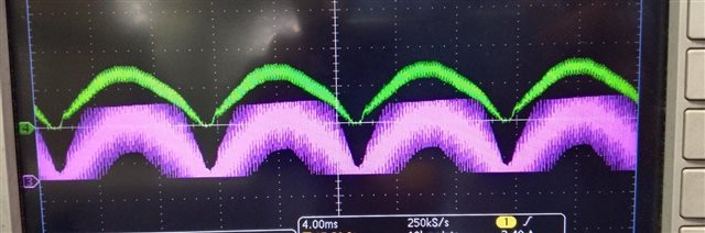
I captured waveforms during startup showing the DC bus ramping up to 440 V, followed by a drop. I also captured the IGBT VCE (yellow) and inductor current (blue) during this period. The PFC operates for about 2–5 seconds, after which the DC voltage drops to Nominal Voltage.

Inductor Current Ringing:

The inductor has a value of 550 µH at 10 A, shunt - 8.6mOhm(Is it very Low). I observe significant ringing in the inductor current. Currently, no snubber is applied to the IGBT switch, assuming the no-load condition would not require it. However, I suspect that the ringing might still be contributing to instability or noise-related issues.

1. Could the Vsense voltage drop be caused by a lack of load (zero current draw), or is there a minimum impedance requirement for the feedback network that I might be missing?

2. Is the observed ringing in the inductor current a concern even under no-load conditions, and should I consider adding a snubber or damping network regardless of load state?

IGBT Sw & Inductor current

  • Hello Shalini, 

    Normally, the VSENSE voltage does NOT drop to 0V after 2~3 seconds, regardless of load or no load.  VSENSE should be a simple resistor divider from Vout.  If your VSENSE is doing this, some thing attached to the VSENSE net is causing it.  It would be very helpful to provide the schematic diagram to see what could be affecting VSENSE in this way. 

    The waveforms show a DC bus voltage of ~90V, which is not the usual "nominal" output voltage.  
    The blue inductor waveform is AC coupled and inverted.  Please use DC coupling and show positive current. 

    Actually the DC voltage looks too flat to be real.  
    I suspect that you are using a probe or an oscilloscope channel that has limited voltage capability and is clamping to ~90V. 
    Also, I think you are using a 50/60Hz current probe which cannot show high frequency inductor currents. 
    Notice that the "ringing current" in the inductor is about 100Hz, which is not the switching frequency.   This is not ringing, but distortion by the probe. 
    Please be sure to use probes that are suitable for high voltage and high frequency. 

    Also, please provide the input and output voltage design targets for your project. 
    Better yet, please provide the Excel worksheet with your design inputs.

    Edited reply: Also, please increase your oscilloscope sample resolution from 25kS/s to 250MS/s, if possible.  40us per sample is not sufficient to view switching signals. 

    Regards,
    Ulrich

  • Hello Mr. Ulrich,

    Thanks for the reply, I will check on the inputs you have provided, I have attached the calculation sheet, and Schematic, please verify the values and I want to let you know the V-sense is fluctuating and then it is dropping to mV during High voltage after some time, this itself making the system more unstable.

    Last time I tested while the DC bus voltage is shoot above 440VDC at 200VAC input, because the Vsense is not stable, The IC got failed none other than the Vsense pin is showing low impedance of below 20Ohm with respect to IC GND pin. (Note: I'm probing the Vsense Pin without even turning ON the IC, without IC the sensing voltage is perfect with IC it is dipping even when the IC is not turned ON)

    And with respect to Vsense resistor divider I have checked it seperately upto 450V and the divider network is providing the calculated voltage on the respective node.

    Please review these values and let me know the selected values need to be changed,

    Thanks.

  • Hello Ulrich,

    I have attached the Excel worksheet and schematic in the previous reply,

    I have tested with the provided inputs, the output looks like the signals attached in this reply, Pink(VBUS Output), Blue(VCE - Across IGBT) and Yellow(I_L - Inductor current) with higher resolution, still the behaviour is same, upto some input voltage there is no problem with Vsense, then it starts dropping,

    The initial startup looks like it tries to start switching, then it stops due to some feedback error I suspect,

    share your feedback,

    Thanks.

  • Please give us some time to get back to you

  • Hello Shalini, 

    Sorry I was out of office for some time.  I don't see anything of major concern in the schematic design.  I think  C35 = 10000pF at ICOMP is a little high, and I suggest to reduce to 6800pF. 

    The waveforms are difficult to view when posted sideways as shown above.  

    The 4th waveform shows VBUS at <300V and hardly rising during the switching before the switching stops. 
    The 3rd waveform shows significant DCM in the switching, so very little power is being delivered. 

    Do you have a load on the PFC output during start-up?  

    If VSENSE falls to 0V and you measure ~20R to GND instead of 12.7kR, then I think the IC input is getting damaged. 
    Maybe there is ESD damage during probing.  

    As I mentioned before, the schematic design looks okay, so the problem must be in the board. 
    Please review your PFC design on the board and make sure it is connected as the schematic shows and that the component values are as the schematic shows. 

    Regards,

    Ulrich

  • Hi Ulrich,

    Thanks for the feedback, I have tested up-to 1.2kW and the efficiency is 99%, and the waveform looks fine, Please verify and let me know the waveform is OK.

    Thanks.