


Other Parts Discussed in Thread: BQSTUDIO
Tool/software:
Hi Technical Experts,
I hope you are having a great day.
I am currently using the BQ7695202 AFE with an NXP MCU, and I have successfully read the cell voltages and internal temperature. However, I am encountering issues with reading the external temperature, as I am consistently getting a temperature reading of 0.
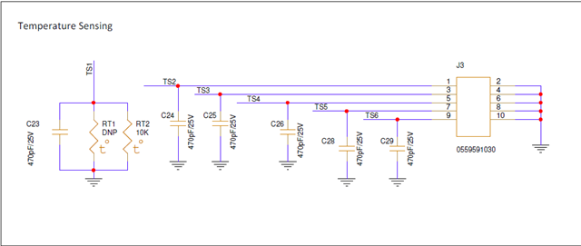
I am using a 10 kΩ temperature sensor.
I would greatly appreciate it if you could provide any sample code that facilitates the reading of data from an external temperature sensor. Such assistance would be invaluable to my work.
This is the schematic part of temperature sensor.
And this is my init part of my code :
void BQ769x2_Init()
{
// Configures all parameters in device RAM
// Enter CONFIGUPDATE mode (Subcommand 0x0090) - It is required to be in CONFIG_UPDATE mode to program the device RAM settings
// See TRM for full description of CONFIG_UPDATE mode
CommandSubcommands(SET_CFGUPDATE);
// After entering CONFIG_UPDATE mode, RAM registers can be programmed. When programming RAM, checksum and length must also be
// programmed for the change to take effect. All of the RAM registers are described in detail in the BQ769x2 TRM.
// An easier way to find the descriptions is in the BQStudio Data Memory screen. When you move the mouse over the register name,
// a full description of the register and the bits will pop up on the screen.
// 'Power Config' - 0x9234 = 0x2D80
// Setting the DSLP_LDO bit allows the LDOs to remain active when the device goes into Deep Sleep mode
// Set wake speed bits to 00 for best performance
BQ769x2_SetRegister(PowerConfig, 0x2D80, 2);
// 'REG0 Config' - set REG0_EN bit to enable pre-regulator
BQ769x2_SetRegister(REG0Config, 0x01, 1);
// 'REG12 Config' - Enable REG1 with 3.3V output (0x0D for 3.3V, 0x0F for 5V)
BQ769x2_SetRegister(REG12Config, 0x0D, 1);
// BQ769x2_SetRegister(CFETOFFPinConfig, 0x00, 1);
// Set DFETOFF pin to control BOTH CHG and DSG FET - 0x92FB = 0x42 (set to 0x00 to disable)
BQ769x2_SetRegister(DFETOFFPinConfig, 0x00, 1);
// Set up ALERT Pin - 0x92FC = 0x2A
// This configures the ALERT pin to drive high (REG1 voltage) when enabled.
// The ALERT pin can be used as an interrupt to the MCU when a protection has triggered or new measurements are available
BQ769x2_SetRegister(ALERTPinConfig, 0x2A, 1);
// Set TS1 to measure Cell Temperature - 0x92FD = 0x07
BQ769x2_SetRegister(TS1Config, 0x07, 1);
// Set TS3 to measure FET Temperature - 0x92FF = 0x0F
BQ769x2_SetRegister(TS3Config, 0x07, 1);
// Set HDQ to measure Cell Temperature - 0x9300 = 0x07
BQ769x2_SetRegister(HDQPinConfig, 0x0B, 1); // No thermistor installed on EVM HDQ pin, so set to 0x00
// Set HDQ to measure Cell Temperature - 0x9300 = 0x07
BQ769x2_SetRegister(CFETOFFPinConfig, 0x03, 1); // No thermistor installed on EVM HDQ pin, so set to 0x00
// Set HDQ to measure Cell Temperature - 0x9300 = 0x07
BQ769x2_SetRegister(DCHGPinConfig, 0x0B, 1); // No thermistor installed on EVM HDQ pin, so set to 0x00
// Set HDQ to measure Cell Temperature - 0x9300 = 0x07
BQ769x2_SetRegister(DDSGPinConfig, 0x0B, 1); // No thermistor installed on EVM HDQ pin, so set to 0x00
// 'VCell Mode' - Enable 16 cells - 0x9304 = 0x0000; Writing 0x0000 sets the default of 16 cells
BQ769x2_SetRegister(VCellMode, 0x0000, 2);
// Enable protections in 'Enabled Protections A' 0x9261 = 0xBC
// Enables SCD (short-circuit), OCD1 (over-current in discharge), OCC (over-current in charge),
// COV (over-voltage), CUV (under-voltage)
BQ769x2_SetRegister(EnabledProtectionsA, 0xBC, 1);
// Enable all protections in 'Enabled Protections B' 0x9262 = 0xF7
// Enables OTF (over-temperature FET), OTINT (internal over-temperature), OTD (over-temperature in discharge),
// OTC (over-temperature in charge), UTINT (internal under-temperature), UTD (under-temperature in discharge), UTC (under-temperature in charge)
BQ769x2_SetRegister(EnabledProtectionsB, 0xF7, 1);
// 'Default Alarm Mask' - 0x..82 Enables the FullScan and ADScan bits, default value = 0xF800
BQ769x2_SetRegister(DefaultAlarmMask, 0xF882, 2);
// Set up Cell Balancing Configuration - 0x9335 = 0x03 - Automated balancing while in Relax or Charge modes
// Also see "Cell Balancing with BQ769x2 Battery Monitors" document on ti.com
BQ769x2_SetRegister(BalancingConfiguration, 0x03, 1);
BQ769x2_SetRegister(CCGain, 0xF2416F41, 4);// 0x416f41f2 = F2416F41
// Set up CUV (under-voltage) Threshold - 0x9275 = 0x31 (2479 mV)
// CUV Threshold is this value multiplied by 50.6mV
//writing 0x31 decimal 49 threshold voltage = 49 × 50.6 mV = 2479.4 mV
BQ769x2_SetRegister(CUVThreshold, 0x31, 1);
// Set up COV (over-voltage) Threshold - 0x9278 = 0x55 (4301 mV)
// COV Threshold is this value multiplied by 50.6mV
BQ769x2_SetRegister(COVThreshold, 0x55, 1);
// Set up OCC (over-current in charge) Threshold - 0x9280 = 0x05 (10 mV = 10A across 1mOhm sense resistor) Units in 2mV
BQ769x2_SetRegister(OCCThreshold, 0x05, 1);
// Set up OCD1 Threshold - 0x9282 = 0x0A (20 mV = 20A across 1mOhm sense resistor) units of 2mV
BQ769x2_SetRegister(OCD1Threshold, 0x0A, 1);
// Set up SCD Threshold - 0x9286 = 0x05 (100 mV = 100A across 1mOhm sense resistor) 0x05=100mV
BQ769x2_SetRegister(SCDThreshold, 0x05, 1);
// Set up SCD Delay - 0x9287 = 0x03 (30 us) Enabled with a delay of (value - 1) * 15 µs; min value of 1
BQ769x2_SetRegister(SCDDelay, 0x03, 1);
// Set up SCDL Latch Limit to 1 to set SCD recovery only with load removal 0x9295 = 0x01
// If this is not set, then SCD will recover based on time (SCD Recovery Time parameter).
BQ769x2_SetRegister(SCDLLatchLimit, 0x01, 1);
// Exit CONFIGUPDATE mode - Subcommand 0x0092
CommandSubcommands(EXIT_CFGUPDATE);
}
Thank you for your support. If you required any other informations kindly let me know.
Best regards,
Janakiraman S
