TPS923652: Verifying max switching frequency based on minimum off-time

Part Number: TPS923652
Other Parts Discussed in Thread: TPS61165

Tool/software:

Hello,

I'm designing a Boost LED driver using the TPS923652, and I would like to confirm that my chosen switching frequency is safe with respect to the controller’s minimum off-time requirement.

Design specification:

  • VOUT: 25.6 V

  • VIN range: 6.0 V to 8.4 V (2S Li-ion)

  • Minimum off-time (datasheet): 100 ns

  • Design margin on Toff: +30% → 135 ns minimum used in calculations

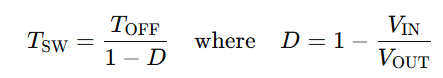
To ensure I'm within safe operating limits, I computed the required switching period from the off-time constraint using the formula:

Using the worst-case condition (highest duty cycle at VIN = 6.0 V):

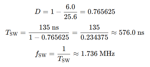
So, to maintain a 135 ns minimum off-time, the maximum safe switching frequency should be ~1.74 MHz.

With Rfset = 18kOhm I choose 1.5MHz.

My questions are

  1. Can you confirm that this reasoning is valid and that the calculations are correct?
  2. Is there any additional timing margin you would recommend (e.g., more than 30%) to account for internal tolerances or variations?

Thank you for your support.

Best regards,
Thomas

  • Hi Thomas,

    Pls kindly let me check your question and get back to you during these days. Thank you!

    BRs

    Lucia

  • Hi Lucia,

    I’m following up on my question from last week regarding the TPS923652 switching frequency and minimum off-time margin.

    Have you had a chance to review my calculations?

    Additionally, I have another related question:


    When selecting the Schottky diode for this type of LED driver, I could not find detailed guidance in the TPS923652 datasheet. However, in another datasheet (TPS61165), TI states:

    Ensure that the average and peak current rating of the diode exceeds the average output current and peak inductor current. In addition, the reverse breakdown voltage of the diode must exceed the open LED protection voltage.

    Are there any other key parameters I should consider for optimal diode selection in this application ?

    Thank you for your time and support.

    Best regards,
    Thomas

  • Hi Thomas,

    For the selection of the switching frequency, besides the minimum off time, another thing that should take into consideration is the thermal performance:

    (1) Switching frequency: For your calculations, they are almost good, but one thing need to mention here is that the duty cycle is also be related with the efficiency. In ideal case, D=1-VIN/VOUT; However, actually D=1-VIN*Eff/Vout. For example, you can use 80% as a start point. For the min off time margin, there is no high limit data here. I would suggest you can leave +100% margin to ensure good operation.

    (2) Thermal performance: Different switching frequency will result in different switching losses. And the thermal performance will also be related with different copper thickness, layout and vias. Thus, I would recommend you can first check with TPS923652EVM board and also verify with your board.

    Thank you!

    BRs

    Lucia

  • Hi Lucia,

    Sorry for the late reply.

    I have updated my calculations by taking into account the efficiency and the +100% margin as you suggested.
    I also noted your comments regarding the thermal performance considerations.

    However, I haven’t received feedback yet regarding the diode selection from my previous message. Could you please confirm the main parameters to consider?

    In addition, I would like to confirm if it is acceptable to directly connect the VCC pin to the EN/PWM pin in order to indicate analog PWM mode.

    Finally, would it be possible to request a schematic review once my design is completed?

    Thank you again for your support.

    Best regards,
    Thomas

  • Hi Thomas,

    You can connect to Vcc with a pull up resistor. For the diode selection, pls kindly let me check if we have any material to share with you. Yes, we can review the design.

    Thank you!

    BRs

    Lucia

  • Hi Lucia,

    Thank you for your reply.

    I just wanted to kindly follow up regarding the diode selection — have you been able to find any material to share with me on this topic?

    Also, would it be possible to send you my schematic and layout in a private message for review? The project is currently designed with KiCad — do you have the possibility to open KiCad files directly, or would you prefer that I provide screenshots instead?

    Thanks again for your support.

    Best regards,
    Thomas

  • Hi Thomas,

    Sorry for late as I have limited bandwidth recently. Pls allow me some time but I'll share with you before end of this week. Thank you for your understanding!

    BRs

    Lucia

  • Hi Lucia,

    I just wanted to kindly follow up regarding the diode selection material, as well as the possibility to send you my schematic and layout for review.
    No rush if you are still busy — I just wanted to check if you had any updates.

    Best regards,
    Thomas

  • Hi Thomas,

    The rectifier is to carry the inductor current during t_OFF. The most efficient choice for D1 is a Schottky diode due to low forward voltage drop and near-zero reverse recovery time. Recommend to have a voltage rating >15% of the input voltage to ensure safe operation during the ring of the switch diode. Current rating > 15% higher than the average diode current. Id=(1-Dmax)* IL. The diode should be sized to exceed the current rating, and the package should be able to dissipate power without exceeding the maximum allowable temperature.

    Thank you!

    BRs

    Lucia

  • Hi Lucia,

    Thank you for your detailed explanation regarding the diode selection — I have noted your recommendations.

    As a final request, would it be possible to have a schematic and layout review of my design? Please let me know if you prefer KiCad files directly or screenshots instead.

    Best regards,
    Thomas

  • Hi Thomas,

    Pls kindly send to my email (lucia-gao@ti.com) Thank you!

    BRs

    Lucia