TPS59641: Noise Spikes on GPU Phase

Part Number: TPS59641

Tool/software:

Hi, 

I have already developed a custom board with Intel Atom E3826 (Bay Trail) which is being powered ON by TPS59641 multiphase VR (SVID, IMVP7).

The operating conditions are- 

Parameter CPU GFX Unit
Number of phases 1 1
VID_Vcore_HFM (0 A) 1.0000 1.0000 V
R_Loadline 5.9 5.9 mV/A
Maximum Current (Icc_max) 4 10 A
Per phase Maximum Current 4.0 10.0 A
Thermal Design Current (I_TDC_total) 2 5 A
Per phase Thermal Design Current 2.0 5.0 A
SetVID Fast Slew Rate (Typical) 12 mV/µs
Load Current for Bode Plot 4 10 A
Vin max 5.5 V
Vin min 4.5 V
Frequency (Freq) 500 605 kHz
Minimum Recommended Inductance 1.02 0.34 µH
Maximum Recommended Inductance 2.05 0.68 µH
Chosen Inductance, L 1.5 0.68 µH
Inductor DCR (L_DCR) 5.700 5.000

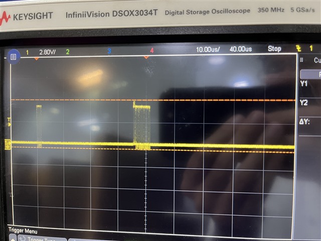
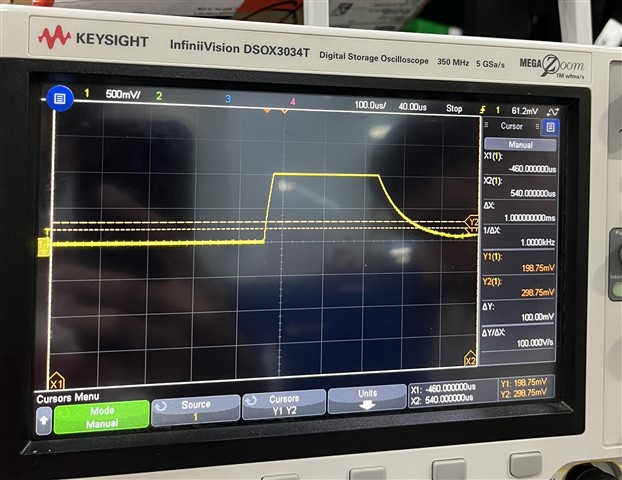
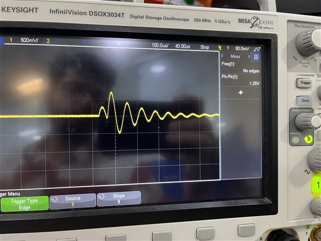
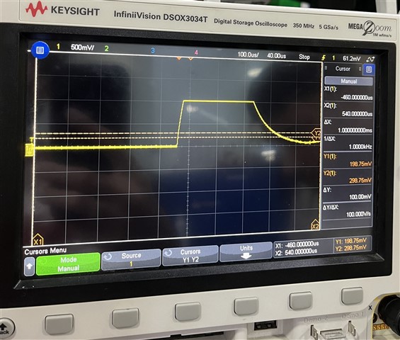
Please find the attached Schematic and captured waveform (ac biased) for your reference.

Problem Statement: While probing the GPU phase ripples, We are observing some 50mV to 55mV peak to peak switching noise kind of thing. Please refer the attached schematic and do let us know what can be suggested to mitigate the noise. 

6560.SCHEMATIC1 _ PAGE1.pdf

Thank You

Raj Kumar

  • Hi Raj,

    An expert will answer you by tomorrow.

    Regards,

    Maha

  • Hi Maha,

    Thank you so much for the consideration and notifying the expert.

    Regards,

    Raj

  • Hi Raj,

    As per my understanding from your question, you are including the spikes on output voltage while measuring the peak to peak ripple on output. That is switching noise getting  coupled to probe. Please use a probe bandwidth of 20Mhz setting on Scope, while measuring the peak to peak ripple on output voltage. To verify, if it is switching noise or not please probe PWM also along with VOut.

    Best Regards,

    Chanakya.  

  • Hello Chanakya,

    Thank you so much for the suggestions and information.

    Yes, after enabling the oscilloscope limit. It got cleared. so, it was coupled noise with probe only.

    Thanks 

    Raj

  • Hi Raj,

    Thank you for the confirmation. I'm closing this thread.

    Best Regards,

    Chanakya.

  • Hello Chanakya,

    I request you not to close the thread, as I am facing another issue in the same circuit (please refer to the initially shared schematic page and input/output parameters).

    Problem statement:
    The TPS59641RSLT is not generating the VCC (CPU) channel voltage, although the VNN (GPU) voltage of 1.1 V (VBOOT) is being generated on one of our 20 custom boards. We have recently encountered this issue; earlier it was working as expected.

    To debug this, we have followed these steps:

    1. Replaced inductor L56 and output capacitors – no improvement.

    2. Disconnected the load (processor supply bank) from the source VRM – no improvement.

    3. Checked the circuitry and component values on CF-IMAX, CIMON, CTHERM, COCP-I, and CCSP1/CCSN1; also replaced the components – no improvement.

    4. Verified V5DRV and other 3.3 V/5 V input supplies – all okay.

    When probing the CSW1 pin of the VRM, I observe square waves (5 V amplitude) for a short duration (approx. 60 µs).
    Similarly, probing the VSW pins of the power MOSFET (U138) shows the same square wave pulses for the same duration.

    However, there is no output voltage spike on the VCC_DCD0 power nets.

    I suspect this may be due to an overcurrent error, UVP, thermal error, or some other fault condition. To investigate further, I probed the CIMON pin and observed a 1.05 V spike for a short duration, which could indicate an overcurrent condition—even though no load is connected.

    Attached are the CSW1, VSW, and CIMON waveforms for your reference.
    I kindly request your help in diagnosing and resolving this issue.

    Thanks 

    Raj 

  • Hi Raj,

    From your observations ,It gives an impression like the feedback from output voltage is not reaching the TPS59641. Please can you check the feedback  network. Also can you check the voltage level on switch node, if you are getting some pulses on switch node there should be some raise in the output voltage. Please give us sometime to go through this issue , this part is a very old part..

    Best Regards,
    Chanakya.

  • Hello Chanakya,

    Thank you for the response.

    I have checked the continuity on feedback pins "CVFB" & "CGFB", and it okay. There is nothing much in feedback path except the 10-ohm series register. 

    Additionally, I have replaced the components in current sense circuit "CCSP1" and "CCSN1". It didn't solve the issue.

    Since, we are getting the 5V pulses on VSW pins of MOSFET for short duration, Ideally we should have get some voltage buildup. but a few days back, we observed this kind of waveform on the output stage. refer to the below image- (this is the VOUT when load is disconnected)-

    Thank You

    Raj Kumar

  • Hi Raj,
    Please can you probe VOut and switching node together

    Best Regards,
    Chanakya.

  • Hi Chanakya,

    Sure, I will do that.

    There is a holiday tomorrow. I will take the observation the day after tomorrow.

    Thanks

    Raj

  • Hi Raj,

    Thank you, that helps.

    Best Regards,
    Chanakya.

  • Hello Chanakya,

    Apologies for the delayed response—some urgent tasks pulled me away.

    Per our discussion, I probed VSW and VOUT simultaneously:

    • Probe 1: VSW

    • Probe 2: VOUT

    Please find the latest waveform attached for reference.

    Observation: Previously, the VSW pulse persisted for ~400 µs before dying out, then reduced to ~60 µs, and now it’s down to ~2–3 µs.

    Please find the attached latest waveform.

    Regards,

    Raj

  • sorry for the repetitive images in above message due to some technical error.

  • Hi Raj,

    It's not clear from the pictures, please can you store the scope shot and send the jpg file.

    Best Regards,

    Chanakya.

  • Hello Chanakya,

    I carried out an activity to evaluate how well the VR and MOSFET switch under free-running conditions (with the inductor and NTC sense circuit removed).

    In this setup, I observed that the MOSFET generates 5 V square pulses at the VSW pins, lasting for approximately 800 µs.

    After re-populating the inductor and NTC sense circuit, I probed the VSW pins again and observed that the switching time dropped significantly—from about 800 µs to 3 µs.

    Please find the attached waveforms for your reference.

    FREE RUNNING SWITCHING (WITHOUT INDUCTOR)

    VSW WITH INDUCTOR 

    I hope this observation help us to understand the issue better.

    Thanks 

    Raj

  • Hi Raj,

    Is this issue repeatable on multiple boards?

    Best Regards,
    Chanakya.

  • Hi Chanakya,

    This is the first time we are facing this issue in the last three years. Out of 15 boards from the same batch, only one has been exhibiting this problem for the past two months.

    Regards,

    Raj

  • Hi Raj,

    Please can you try swapping this part with a part on working board. Please let us know if the issue still persists, we want to do this exercise to find out whether the issue is related to Board or part.

    Best Regards,
    Chanakya

  • Hi Chanakya,

    Swapping the IC is not easy due to the high board density.

    I have an observation:

    When I probed the CIMON (CPU Phase Current Monitor Pin), it showed a logic high for about 250 µs. Is this normal behavior, or does it indicate a high current issue during startup or some other error?

    Please refer to the attached waveform for reference.

    Regards,

    Raj

  • Hi Raj,

    Swap test is important to identify if it's the board issue or device issue. As this part is designed 15 years back in TI, we have limited information on this part, doing swap test will help us a lot in debug.

    Please plan to do the swap test, meanwhile I will collate the information in e2e regarding the issue and check with my team members.

    Best Regards,
    Chanakya.