

Other Parts Discussed in Thread: TPS25947
Tool/software:
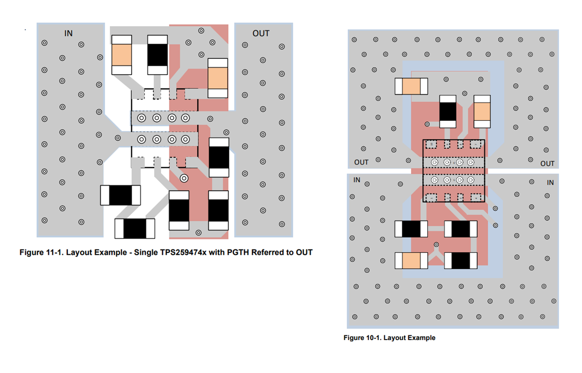
Hello all,
I’m using the TPS22811 and TPS25947 in two different projects, and I noticed that the recommended layout examples for these two parts (Figures 10-1 and 11-1 in their respective datasheets) use very different VIN/VOUT routing strategies:
-
The TPS22811 layout shows VIN/VOUT being routed into the IC from two separate traces on opposite sides.
-
The TPS25947 layout routes VIN/VOUT from a single wide connection, entering at only one point.
Since both devices are in a similar WSON/QFN-style package with exposed pads, I’m curious:
-
What is the reason behind using two entry points for VIN/VOUT in one case and a single-point, plane-fed approach in the other?
-
Can the TPS25947 be safely routed using dual-entry like TPS22811, or is single-point recommended to maintain current sense / protection accuracy?
Thanks in advance!
Nir

