


Tool/software:
Hallo,
I have a BQ25620 running and control it via a linux computer.
It works fine except:
- it does not charge the battery, it just powers the system (via battery or via VBUS, if available)
- VBUS stays high after unplugging the USB charger; when I enable EN_HIZ, then USB voltage drops to zero (charger not plugged in).
I was able to verify all ADC values using lab measurement equipment.
19:07:13 - Charging (CC/Pre), IBUS: 392 mA
19:07:13 - Charging (CC/Pre), IBAT: 16 mA
19:07:13 - Charging (CC/Pre), VBUS: 5054 mV
19:07:13 - Charging (CC/Pre), VPMID: 5050 mV
19:07:13 - Charging (CC/Pre), VBAT: 3611 mV
19:07:13 - Charging (CC/Pre), VSYS: 3621 mV
attached the register dumps:
- 00: initial after powering the system from battery only
- 01: after setting
#disable watchdog --> a1 --> a0
set_register_8(bus,0x16,0xa0)# Iprechg to 240mA
set_register_16(bus,0x10,0x00C0)#disable thermal
set_register_8(bus,0x1A,0x80)#disable EN_TERM 0x06 -> 0x02
set_register_8(bus,0x14,0x02)# enable ADC
set_register_8(bus,0x26,0x80)
set_register_8(bus,0x27,0x04) - 02: after plugging in a charger. Charger means Vcc + GND on Lab Power supply, D+ and D- shorted. I can see the VBUS voltage, but I ould expect a high (>1A) charge current. My power supply shows 200mA@5.2V
- 03: after unplugging the charger - VBUS stays at VPMID level. I could clear it by setting EN_HIZ =1 for a short time
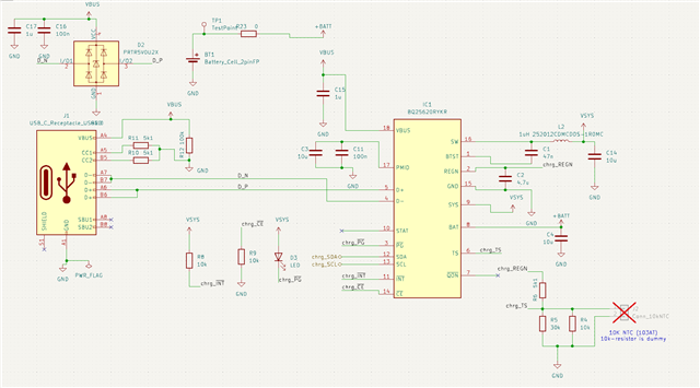
The schematic is attached as screenshot.
Any help or tips appreciated.
* Created: Tue Sep 19 18:57:42 CEST 2023
*
* Format: Register Name  tab Character,	  Register Address  tab Character,	  Hexadecimal register value.
* Device: BQ25620/2
* BQZ Container: Charger_1_00-bq25620)2.bqz
*
REG02_Charge_Current_Limit	0340
REG04_Charge_Voltage_Limit	0D20
REG06_Input_Current_Limit	0A00
REG08_Input_Voltage_Limit	0E60
REG0A_IOTG_Regulation	0320
REG0C_VOTG_Regulation	0FC0
REG0E_Minimal_System_Voltage	0B00
REG10_Pre-charge_Control	0050
REG12_Termination_Control	0030
REG14_Charge_Control	06
REG15_Charge_Timer_Control	5C
REG16_Charger_Control_0	A1
REG17_Charger_Control_1	4F
REG18_Charger_Control_2	04
REG19_Charger_Control_3	C0
REG1A_NTC_Control_0	3D
REG1B_NTC_Control_1	25
REG1C_NTC_Control_2	3F
REG1D_Charger_Status_0	01
REG1E_Charger_Status_1	00
REG1F_FAULT_Status_0	00
REG20_Charger_Flag_0	01
REG21_Charger_Flag_1	00
REG22_FAULT_Flag_0	00
REG23_Charger_Mask_0	00
REG24_Charger_Mask_1	00
REG25_FAULT_Mask_0	00
REG26_ADC_Control	30
REG27_ADC_Function_Disable_0	00
REG28_IBUS_ADC	0000
REG2A_IBAT_ADC	0000
REG2C_VBUS_ADC	0000
REG2E_VPMID_ADC	0000
REG30_VBAT_ADC	0000
REG32_VSYS_ADC	0000
REG34_TS_ADC	0000
REG36_TDIE_ADC	0000
REG38_Part_Information	02
* Created: Tue Sep 19 18:59:10 CEST 2023
*
* Format: Register Name  tab Character,	  Register Address  tab Character,	  Hexadecimal register value.
* Device: BQ25620/2
* BQZ Container: Charger_1_00-bq25620)2.bqz
*
REG02_Charge_Current_Limit	0340
REG04_Charge_Voltage_Limit	0D20
REG06_Input_Current_Limit	0A00
REG08_Input_Voltage_Limit	0E60
REG0A_IOTG_Regulation	0320
REG0C_VOTG_Regulation	0FC0
REG0E_Minimal_System_Voltage	0B00
REG10_Pre-charge_Control	00C0
REG12_Termination_Control	0030
REG14_Charge_Control	02
REG15_Charge_Timer_Control	5C
REG16_Charger_Control_0	A0
REG17_Charger_Control_1	4F
REG18_Charger_Control_2	04
REG19_Charger_Control_3	C0
REG1A_NTC_Control_0	80
REG1B_NTC_Control_1	25
REG1C_NTC_Control_2	3F
REG1D_Charger_Status_0	00
REG1E_Charger_Status_1	00
REG1F_FAULT_Status_0	00
REG20_Charger_Flag_0	00
REG21_Charger_Flag_1	00
REG22_FAULT_Flag_0	00
REG23_Charger_Mask_0	00
REG24_Charger_Mask_1	00
REG25_FAULT_Mask_0	00
REG26_ADC_Control	80
REG27_ADC_Function_Disable_0	04
REG28_IBUS_ADC	0000
REG2A_IBAT_ADC	FF18
REG2C_VBUS_ADC	0000
REG2E_VPMID_ADC	0CE4
REG30_VBAT_ADC	0E1E
REG32_VSYS_ADC	0E16
REG34_TS_ADC	0000
REG36_TDIE_ADC	003F
REG38_Part_Information	02
* Created: Tue Sep 19 18:59:41 CEST 2023
*
* Format: Register Name  tab Character,	  Register Address  tab Character,	  Hexadecimal register value.
* Device: BQ25620/2
* BQZ Container: Charger_1_00-bq25620)2.bqz
*
REG02_Charge_Current_Limit	0340
REG04_Charge_Voltage_Limit	0D20
REG06_Input_Current_Limit	04B0
REG08_Input_Voltage_Limit	0E60
REG0A_IOTG_Regulation	0320
REG0C_VOTG_Regulation	0FC0
REG0E_Minimal_System_Voltage	0B00
REG10_Pre-charge_Control	00C0
REG12_Termination_Control	0030
REG14_Charge_Control	02
REG15_Charge_Timer_Control	5C
REG16_Charger_Control_0	A0
REG17_Charger_Control_1	4F
REG18_Charger_Control_2	04
REG19_Charger_Control_3	C0
REG1A_NTC_Control_0	80
REG1B_NTC_Control_1	25
REG1C_NTC_Control_2	3F
REG1D_Charger_Status_0	08
REG1E_Charger_Status_1	0B
REG1F_FAULT_Status_0	00
REG20_Charger_Flag_0	08
REG21_Charger_Flag_1	09
REG22_FAULT_Flag_0	00
REG23_Charger_Mask_0	00
REG24_Charger_Mask_1	00
REG25_FAULT_Mask_0	00
REG26_ADC_Control	80
REG27_ADC_Function_Disable_0	04
REG28_IBUS_ADC	00BA
REG2A_IBAT_ADC	0008
REG2C_VBUS_ADC	13DC
REG2E_VPMID_ADC	13D8
REG30_VBAT_ADC	0E30
REG32_VSYS_ADC	0E3A
REG34_TS_ADC	0000
REG36_TDIE_ADC	005E
REG38_Part_Information	02
* Created: Tue Sep 19 19:00:04 CEST 2023
*
* Format: Register Name  tab Character,	  Register Address  tab Character,	  Hexadecimal register value.
* Device: BQ25620/2
* BQZ Container: Charger_1_00-bq25620)2.bqz
*
REG02_Charge_Current_Limit	0340
REG04_Charge_Voltage_Limit	0D20
REG06_Input_Current_Limit	04B0
REG08_Input_Voltage_Limit	0E60
REG0A_IOTG_Regulation	0320
REG0C_VOTG_Regulation	0FC0
REG0E_Minimal_System_Voltage	0B00
REG10_Pre-charge_Control	00C0
REG12_Termination_Control	0030
REG14_Charge_Control	02
REG15_Charge_Timer_Control	5C
REG16_Charger_Control_0	A0
REG17_Charger_Control_1	4F
REG18_Charger_Control_2	04
REG19_Charger_Control_3	C0
REG1A_NTC_Control_0	80
REG1B_NTC_Control_1	25
REG1C_NTC_Control_2	3F
REG1D_Charger_Status_0	04
REG1E_Charger_Status_1	0B
REG1F_FAULT_Status_0	00
REG20_Charger_Flag_0	04
REG21_Charger_Flag_1	00
REG22_FAULT_Flag_0	00
REG23_Charger_Mask_0	00
REG24_Charger_Mask_1	00
REG25_FAULT_Mask_0	00
REG26_ADC_Control	80
REG27_ADC_Function_Disable_0	04
REG28_IBUS_ADC	0000
REG2A_IBAT_ADC	0008
REG2C_VBUS_ADC	1268
REG2E_VPMID_ADC	1260
REG30_VBAT_ADC	0E14
REG32_VSYS_ADC	0E06
REG34_TS_ADC	0000
REG36_TDIE_ADC	0059
REG38_Part_Information	02
