LM2940C: pattern Layout

Part Number: LM2940C

Tool/software:

Hi,

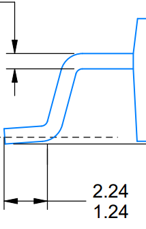
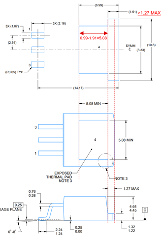
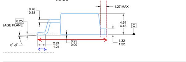
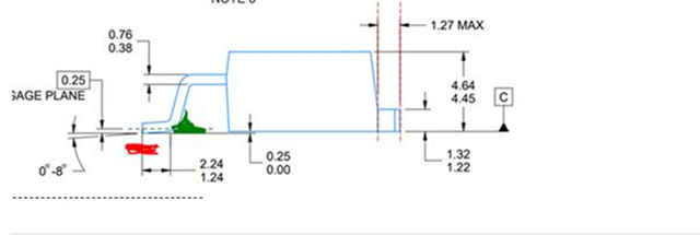
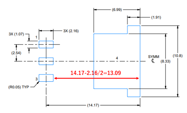
I have a question about the land distance of the TO-263 package. Please tell me the recommended distance of the red line in the data sheet below.

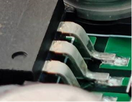
The data sheet states that the distance between the pin and the PAD is 13.09mm. However, in the actual IC, this distance was about 12mm. Therefore, the back fillet of the solder is not formed during mounting.

Best Regards,

Nishie

  • Hi Nishie,

    Thank you for asking us! The concern here is that there is 1mm of variation allowed in the bottom part of the lead. The references have been sized to accommodate the maximum allowed length. 

    Can you show me which points specifically you're measuring the distance between on the IC? And how are you lining up the IC to the pad? The 13.09mm number you calculated is what I would normally recommend. Note that the rightward end of the PCB pad isn't guaranteed to line up with the edge of the IC. I lined up the images below to illustrate the point:

    I would expect the distance between rightward edge of the lead pad to the rightward edge of the PCB thermal pad to be smaller than the actual distance between the elbow of the lead and the far edge of the IC's thermal pad.

    Best,

    Gregory Thompson

  • Hi Gregory-san,

    Thank you for your support.

    ■About the measurement points of the IC
    I measured the red and blue lines in the figure below. The red line is 14.2mm and the blue line is 2mm.

    Therefore, the position of the pad with respect to the IC is the position of the red line in the figure below. Ideally, we think that a fillet like the green line is formed, but in reality, the condition is as shown in the photo. Therefore, we think that the length of the pattern layout does not match the length of the IC.

    ■Regarding the position of the pad and the IC

    I aligned both the left edge (lead side) and the right edge (body side) of the PAD and the IC. However, in either case, the condition is as shown in the above photo.

    Best Regards,

    Nishie

  • Hi Nishie-san,

    The footprint seems to be lined up such that the edge of the leads is on the middle of the pads in both the layout examples and your solder example. I believe this is the source of it. The layout of the pads is designed so that all parts within the controlled dimensions can have a contact, not necessarily that they will form a fillet.

    Aligning the edge of the leads to the far edge of the lead pads or extending the lead pads 1.16mm toward the body will ensure that the inflection point from the bottom part of the leads is close to/over the pad (which is what is preventing the fillet from forming). 

    Best,

    Gregory Thompson

  • Hi Gregory-san,

    The layout of the pads is designed so that all parts within the controlled dimensions can have a contact, not necessarily that they will form a fillet.

    ->Please let me confirm the intention of your answer. Is it correct to understand that a back fillet is not always designed to be formed on the IC lead, and even if a back fillet is not formed, there is no problem with the joint strength?

    Aligning the edge of the leads to the far edge of the lead pads or extending the lead pads 1.16mm toward the body will ensure that the inflection point from the bottom part of the leads is close to/over the pad (which is what is preventing the fillet from forming). 

    ->I aligned the end of the lead with the far end of the lead pad, but it returns to a fixed position due to self-alignment of the reflow. I think I can reduce the effect of self-alignment by reducing the amount of solder very much, but is this action recommended?

    Best Regards,

    Nishie

  • Hi Nishie-san,

    Correct, the recommended layout does not guarantee the formation of a back fillet. A reliable connection may be made without the back fillet formed. The thermal pad is responsible for nearly all the structural connection, so the fillet on the leads is not critical as they do not contribute heavily. The join strength should still be adequate without the back fillet. A good electrical connection will exist in either case. 

    I do not recommend reducing the solder amount on the thermal pad because that controls thermal performance and structural strength. It is better to let the back fillet on the leads remain unformed. I do not foresee that extending the lead pads inward would significantly affect self-alignment, so if a back fillet is still desired, this is likely the best solution. 

    Best,

    Gregory Thompson