This thread has been locked.

If you have a related question, please click the "Ask a related question" button in the top right corner. The newly created question will be automatically linked to this question.

TPSM33625: Regarding DC1 shorting Issue

Part Number: TPSM33625

Tool/software:

Hello Team,

we have initiated one thread over etoe as follow:

 TPSM33625: TPSM33625RDNR 

In that we have below observation

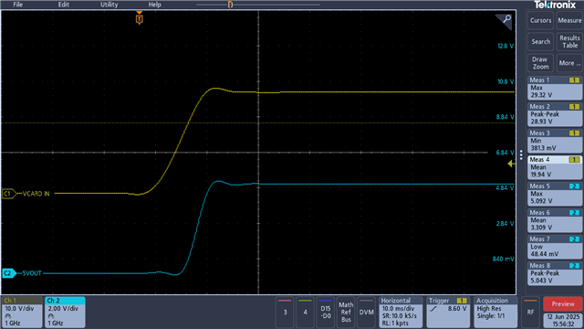
Please find an attached requested input and output voltage and inrush current waveforms which we have captured during panel testing. 
We have found observation as follow:
With the partially DC1 assembled board we are able to damage DC1 with the panel supply.
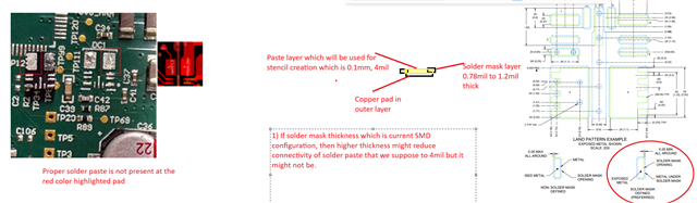
Observation: Upon the removal of soldering from the damaged Dc1 chipset, we found a lack of solder paste on the pad highlighted in red. Additionally, we have reviewed the solder mask guidelines for both the SMD and NSMD configurations as detailed below. (We follow SMD configuration for the solder mask of DC1 chipset)
Stencil which we have used, its thickness is 4mills and solder mask thickness we follow for this batch is in range of 0.78mils to 1.2mils.
We have doubt that because of 1.2mil Solder mask covering pad in "Solder mask defined" configuration, effective paste for DC1 pad will be less, also other components having NSMD configuration where solder mask is 2mil far from copper pad so there is a chance of gap between actual applied paste and DC1 pad is higher and it's causing such dry solder for DC1 pads. 
  • Hello,

    What is the problem with the device?

    If there is no solder on the device, then this may be an issue with the PCB assembly.

    Best regards,

    Ridge

  • Hello Ridge,

    Due to SMD configuration for the solder mask, Solder mask layer is less than the actual pad size. 

    Right now, we have faced some issue of shorting of chipset with machine assembly. 8 out of 10 units got short during normal device operation. once we resolder new chipset (Batch code is same) with help of our internal soldering guy then it is working fine. So now we are Tring to find root cause of the issue. as per our previous analysis and observation we are thinking about that can be assembly issue.

    So, our worries are about mass production. For the prototyping we are ok with the manual reassembly of part but what we can do for the mass production of 500 pieces. so can you suggest what kind of changes we can do in our footprint, so we are not getting this type of issue in mass production.

    So, we are expecting design input for the footprint and assembly guideline for the mounting this chipset for the mass production, otherwise we have to change this part with another vendor.

    Waiting for your prompt response for the same.

    Thanks,

    Denish

  • Hi Denish,

    This appears to be an assembly issue. 

    Is the short from Vout to GND or Vin to GND? Have you measured where the short is on a failed board?

    Since the device works OK when soldered by your technician, that means something is happening in the assembly. Have you checked with the PCB manufacturer on their tolerances or if the design violates any rules in their assembly process?

    Have you assembled any boards with this device using the NSMD footprint?

    Best regards,

    Ridge

  • Hi Ridge,

    Q: Is the short from Vout to GND or Vin to GND? Have you measured where the short is on a failed board?

    A: Some time i/p supply getting short and sometime both i/p and o/p supply getting short.

    Q: Have you checked with the PCB manufacturer on their tolerances or if the design violates any rules in their assembly process?

    A: Assembly vendor told us if pad is solder >70% then as per IPC it passes soldering criteria. We see lots of bubbles in assembly. I attaching x-rays images for your reference. And PCB fab vendor is ok with solder mask and pad clearance criteria. They can fabricate it.

    06 - Xray Report.zip

    Q: Have you assembled any boards with this device using the NSMD footprint?

    A: No, currently we don't proceed for the NSMD configuration. But for the next batch we are think of it. Because in SMD configuration we are getting good result in assembly.

    Can you suggest best suitable guideline for the footprint design and assembly guideline for chipset correct assembly?

    Waiting for your prompt response.

    Thanks,

    Denish Limbachia 

  • Hi Denish,

    Thank you for answering my questions.

    I am reaching out to the relevant team for your assembly questions for this specific package and footprint.

    Please allow a week for their reply. I will update this thread when I hear back.

    Best regards,

    Ridge

  • Hello Denish,

    Support for this issue has been taken up directly via email.

    We should continue through that support avenue. 

    Best regards,

    Ridge

  • Hello Ridge,

    We will wait for it.

    Please try share your inputs as soon as possible.

  • Hi Denish,

    Since experts are supporting directly through email, this thread needs to be closed in order to consolidate communication channels.

    Best regards,

    Ridge